

Global Electronic Materials Market Size and Forecast – 2026 To 2033
The global electronic materials market is expected to grow from USD 83.50 Bn in 2026 to USD 127.30 Bn by 2033, registering a compound annual growth rate (CAGR) of 6.4% from 2026 to 2033. The global electronic materials market is driven by increasing advanced packaging requirements. On January 26, 2025, Micron Technology, Inc. announced plans to build an advanced wafer fabrication facility inside the company’s current NAND manufacturing site in Singapore. This new facility represents a planned investment of approximately USD 24 billion over 10 years and is designed to ultimately provide 700,000 square feet of cleanroom space.
Key Takeaways of the Global Electronic Materials Market
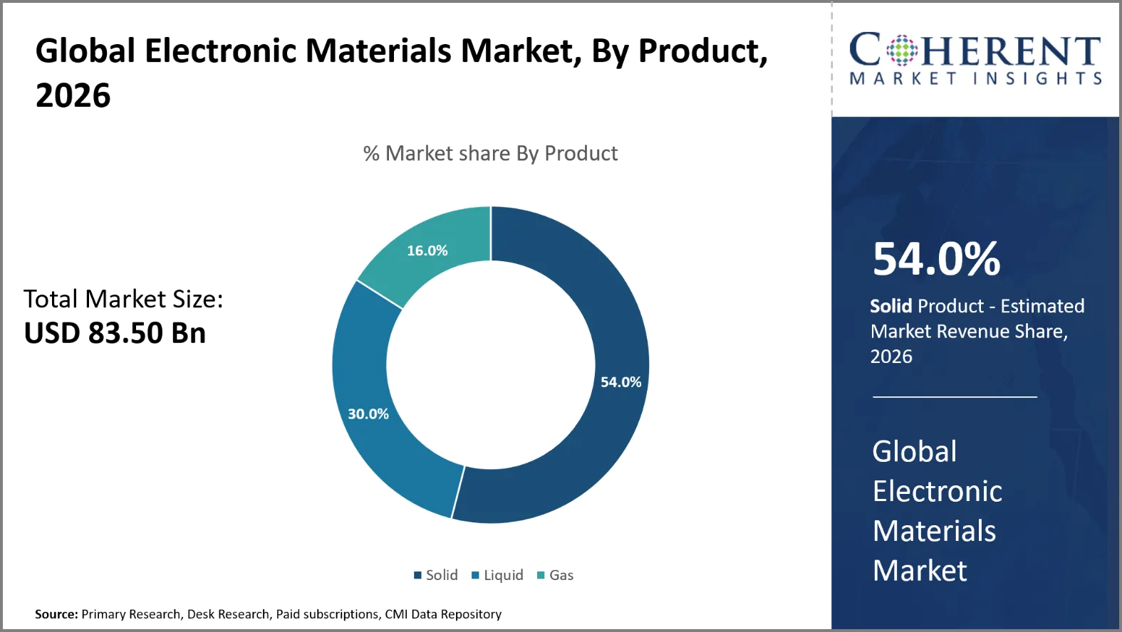
- The Solid segment is expected to account for 54.0% of the global electronic materials market share in 2026. Growing demand for high purity materials is driving the growth of the segment. On March 6, 2026, JX Advanced Metals Corporation announced that it has been installing production facilities at its Ibaraki Office in Japan to meet the growing demand for CVD and ALD materials used in next-generation semiconductors.
- The Silicon Wafers segment is estimated to capture 43.0% of the market share in 2026. Expanding printed circuit board manufacturing is majorly driving the growth of the segment. On September 12, 2025, Panasonic Industry Co., Ltd., a Panasonic Group company, announced plans for a major expansion of its global production capacity for MEGTRON multi-layer circuit board materials.
- The Semiconductors and Integrated Circuits segment is estimated to capture 69.0% of the market share in 2026. Increasing electronic device production is majorly driving the growth of the segment. On October 31, 2025, Samsung Electronics announced plans to create a new AI mega factory in collaboration with NVIDIA. By deploying more than 50,000 NVIDIA GPUs, AI will be embedded throughout Samsung’s entire manufacturing flow, accelerating development and production of next-generation semiconductors, mobile devices and robotics.
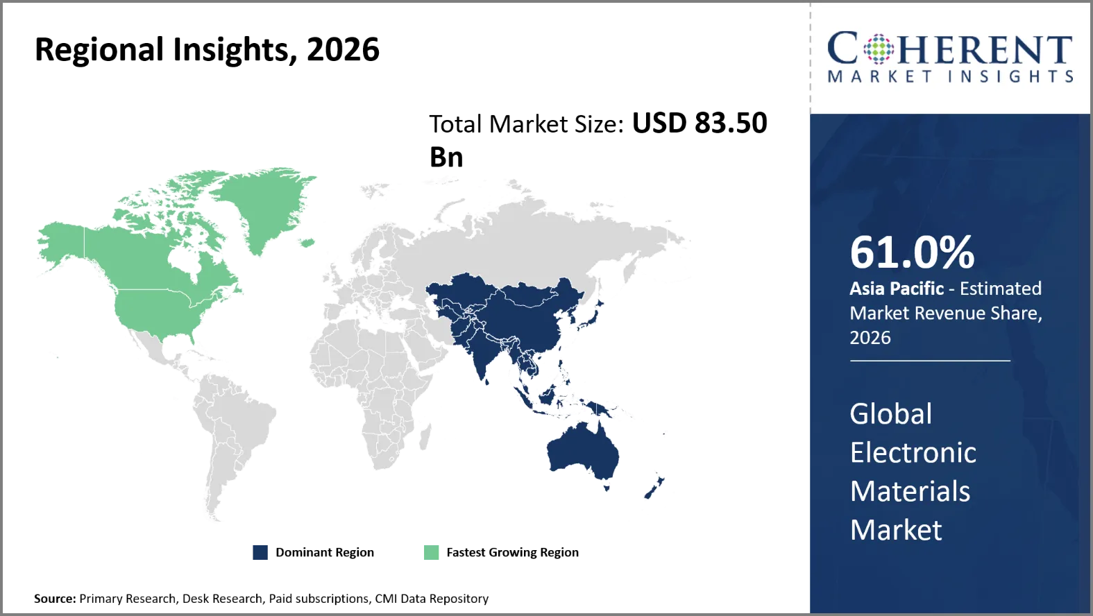
- Asia Pacific is expected to dominate the electronic materials market in 2026 with a market share of 61.0%. Adoption of advanced packaging materials in Asia Pacific is driving the growth of the regional market. On September 9, 2025, Nitto Denko Corporation announced a joint development agreement with IBM to collaborate on advanced packaging technology and materials research.
- North America is expected to account for 20.0% share in 2026 and is projected to record the fastest growth over the forecast period. Growing use of chemical mechanical polishing materials in North America is driving the growth of the regional market. On August 21, 2025, Entegris, Inc., in collaboration with the U.S. Administration, announced USD 700 million in domestic R&D spending over the next several years to accelerate semiconductor innovation.
Segmental Insights
Why Does Solid Dominate the Global Electronic Materials Market?
The solid segment is expected to account for 54.0% of the global electronic materials market share in 2026. Material architectures for semiconductor fabrication depend significantly on stable and finely tailored structures, making solid preferrable. Silicon wafers are the solid substrates on which semiconductor devices and ICs are built. Solid materials have excellent resistance to change in dimension in high temperature processing and repeated chemical treatments. They are also compatible with precise deposition, patterning, etching, doping and metallization procedures. Semiconductor production demands tightly controlled surfaces with known electrical and mechanical properties. Can produce high purity solid electronic materials. Siltronic, for example, spent money to increase its 300-millimeter wafer capacities in 2025 and 2026. In August 2025, their Singapore facility commenced depreciation following large development expenditure. The business said artificial intelligence demand helped sustain larger 300-millimeter wafer quantities in 2025.
- Current Industry Events of 2026
- Market Size Estimation
- Regional Breakdown
- Competitive Landscape
- Customer Intelligence
- Segmental Analysis
- Pricing Analysis
- Key Market Drivers, Challenges & Future Trends
- Customized Insights Section
Why is Silicon Wafers the Most Widespread Application?
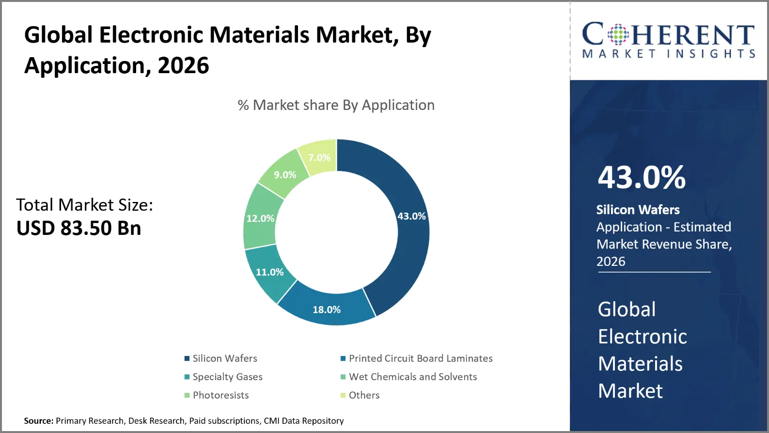
The silicon wafers segment is expected to account for 43.0% of the global electronic materials market share in 2026. Silicon wafers are used widely because silicon has the needed electrical, thermal, and mechanical qualities for semiconductor fabrication. Silicon also has the advantage of sophisticated processing methods and a huge production infrastructure. Its native oxide provides good insulation and surface passivation for semiconductor devices. Silicon wafers are used to manufacture microprocessors, memory devices, sensors and power components. Manufacturers can make silicon wafers of varying diameters and thicknesses for multiple applications. Advanced fabrication procedures also require highly polished and ultra-pure silicon substrates.
On July 9, 2026, Micron Technology, Inc. announced plans to invest up to USD 3 billion to strengthen the U.S. semiconductor supply-chain ecosystem and enable the critical semiconductor manufacturing footprint needed for future technology innovation. As part of Micron’s planned investment into the U.S. supply chain, the company will provide GlobalWafers Co., Ltd. with USD 500 million in strategic financing support to advance the development and manufacturing capabilities of its GlobalWafers U.S. 300mm raw silicon wafer manufacturing facility in Sherman, Texas.
Semiconductors and Integrated Circuits Dominates the Global Electronic Materials Market
The semiconductors and integrated circuits segment is expected to account for 69.0% of the global electronic materials market share in 2026. Semiconductors and integrated circuits require numerous specialized materials throughout device fabrication and packaging. Silicon wafers are used as substrates in producing integrated circuits and semiconductor devices. Photo materials allow exact pattern transfer for high-end lithography operations. Electronic gasses and process chemicals aid deposition, etching, cleaning and doping processes. Packaging materials safeguard semiconductor devices, provide electrical connections, and manage heat. The rising demand for artificial intelligence hardware is fueling the need for better semiconductor fabrication materials. In April 2026, Sumitomo Chemical announced it will build new advanced photoresist technology facility in Osaka, Japan. The facility would combine manufacturing process management, quality assessment and analytical capabilities. It will support advanced logic and memory devices using severe UV and argon fluoride photoresists. Construction is scheduled for completion by fiscal 2027.
Current Events and their Impact
Current Events | Description and its Impact |
European Union - Critical Raw Materials Act, Regulation (EU) 2024/1252 |
|
U.S. - Toxic Substances Control Act Section 8(a)(7) Per- and Polyfluoroalkyl Substances Reporting Rule |
|
Electronic Materials Market Dynamics
Market Drivers
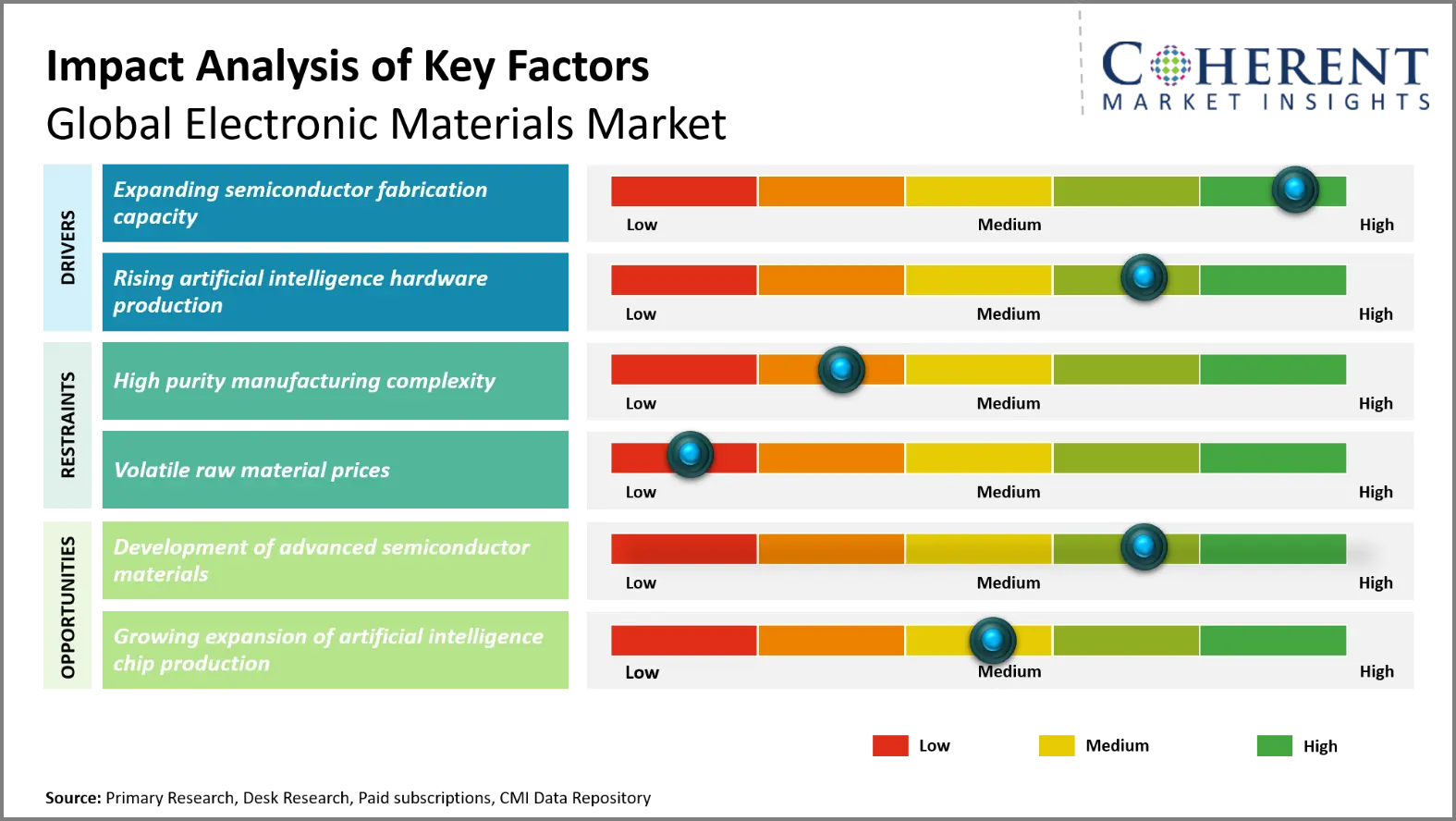
- Expanding semiconductor fabrication capacity: The growth of semiconductor fabrication capacity is driving the demand for specialized electronic materials around the world. New fabs need high-purity silicon wafers, photoresists, specialty gasses, chemicals and innovative packaging materials. Government incentives are fueling domestic semiconductor manufacture in leading technology economies. Leading manufacturers are investing in improved process nodes and larger manufacturing facilities. These investments drive higher material consumption in wafer fab, lithography, deposition, etching and packaging operations. In addition, capacity expansion also pushes material suppliers to build operations closer to semiconductor manufacturing clusters. This tendency reinforces the long-term demand for high purity and application specialized electronic materials.
- On March 4, 2025, TSMC announced plans to expand its investment in advanced semiconductor manufacturing in the U.S. by an additional USD 100 billion. Building on the company’s ongoing USD 65 billion investment in its advanced semiconductor manufacturing operations in Phoenix, Arizona, TSMC’s total investment in the U.S. is expected to reach USD 165 billion.
- Rising artificial intelligence hardware production: Increased artificial intelligence hardware production is driving use of advanced electronic materials. Artificial intelligence processors require sophisticated semiconductor architectures, high-bandwidth memory, advanced substrates, and thermal management materials. Increasing accelerator production is raising demand for materials supporting advanced packaging and high-density interconnections. Semiconductor companies are increasing production capacity for supporting the growing need of AI infrastructure. The better performance of the chips also increases the requirements for the materials with better electrical, thermal and mechanical capabilities. Advanced packaging materials are becoming increasingly important as processor power density continues increasing.
- On December 2, 2025, AWS announced the general availability of Amazon Elastic Compute Cloud (Amazon EC2) Trn3 UltraServers powered by the fourth-generation AI chip Trainium3, AWS’ first 3nm AWS AI chip purpose-built to deliver the best token economics for next-generation agentic, reasoning, and video generation applications.
Emerging Trends
- Advanced Packaging Materials: Advanced packaging is increasing demand for specialized substrates, bonding materials, underfills, and thermal interface materials. Chiplets and heterogeneous integration require materials supporting higher interconnect density, improved thermal performance, mechanical reliability, and increasingly complex semiconductor package architectures.
- High-Purity Material Development: Semiconductor manufacturers are requiring higher purity electronic materials for advanced process nodes. To reduce contamination, enhance manufacturing yields and support increasingly advanced semiconductor fabrication processes, suppliers are producing ultra-high-purity chemicals, gasses, silicon materials and deposition precursors.
- Sustainable Material Solutions: With environmental demands increasing, electronic material makers are working on recyclable, lower-impact and resource-efficient material solutions. Companies are enhancing chemical management, material recovery, process efficiency and waste reduction throughout semiconductor fabrication and broader electronic manufacturing operations.
- Compound Semiconductor Materials: Compound semiconductor materials are in high demand for applications such as electric vehicles, telecommunications, power electronics and data centers. Silicon carbide and gallium nitride enable operation at higher temperatures, faster switching and greater power efficiency in increasingly demanding electronic systems.
Regional Insights
Why is Asia Pacific a Strong Market for Electronic Materials?
Asia Pacific is expected to account for a market share of 61.0% in 2026. Asia Pacific benefits from dense semiconductor manufacturing clusters spanning Taiwan, South Korea, Japan, China, and Southeast Asia. Taiwan and South Korea are expanding advanced logic, memory, and packaging capacity. Japan strengthens the regional supply chain through silicon wafers, photoresists, and semiconductor chemicals. Japan holds approximately 53% of global silicon wafer production and about 50% of photoresist production. Taiwan is developing domestic materials for heterogeneous integration, including interposers, conductor connection materials, and low-dielectric-loss materials. Regional growth therefore increasingly reflects advanced packaging, high-bandwidth memory, artificial intelligence processors, and specialized material localization.
Why Does North America Electronic Materials Market Exhibit High Growth?
North America is expected to register the fastest growth with a CAGR of 7.7% over the forecast period and is projected to account for 20.0% of the global electronic materials market in 2026. North America is expanding electronic materials production alongside new semiconductor fabrication and packaging investments. The region had four semiconductor fabrication projects scheduled to begin construction during 2025. The U.S. Department of Commerce announced up to USD 52.1 million for Sumika Semiconductor Materials Texas. The facility is intended to strengthen domestic supplies of semiconductor-grade materials. Hemlock Semiconductor also received up to USD 325 million for a new semiconductor-grade polysilicon facility. The project is expected to create approximately 180 manufacturing jobs and over 1,000 construction jobs. These investments strengthen regional supplies of polysilicon, specialty chemicals, and other fabrication inputs. Advanced packaging investments are also increasing demand for substrates and thermal-management materials.
Global Electronic Materials Market Outlook for Key Countries
Why is China Emerging as a Major Hub in the Electronic Materials Market?
China is expanding electronic materials demand through rapid semiconductor fabrication investment and domestic supply-chain development. Chinese chipmakers were expected to increase fabrication capacity by 14% during 2025. Major investments involve Semiconductor Manufacturing International Corporation, Huahong Group, Nexchip, and ChangXin Memory Technologies. China is also implementing its 2025-2026 electronic information manufacturing action plan. The plan specifically addresses integrated circuits, electronic components and materials, intelligent sensors, specialized equipment, and photonics. The policy strengthens domestic development of materials supporting semiconductor and electronic manufacturing. Photonics development provides additional opportunities for optical materials and specialized substrates. Domestic fabrication expansion is also increasing requirements for process chemicals, specialty gases, photoresists, wafers, and packaging materials.
Is U.S. the Next Growth Engine for the Electronic Materials Market?
The U.S. electronic materials growth is increasingly supported by domestic semiconductor supply-chain investments. The U.S. Department of Commerce awarded Hemlock Semiconductor up to USD 325 million for semiconductor-grade polysilicon production. The Michigan project is expected to create approximately 180 manufacturing jobs and more than 1,000 construction jobs. Sumika Semiconductor Materials Texas also received preliminary support of up to USD 52.1 million. The Texas facility will strengthen domestic production of high-purity semiconductor chemicals. Coherent also received proposed support for silicon carbide manufacturing capabilities in Pennsylvania. These projects strengthen domestic supplies of polysilicon, specialty chemicals, and compound semiconductor materials. Artificial intelligence infrastructure and advanced packaging are creating further demand for specialized electronic materials.
Taiwan Electronic Materials Market Analysis and Trends
Taiwan remains a major electronic materials hub because of its advanced foundry and packaging ecosystem. Taiwan remained the world's largest semiconductor materials consumer for the sixteenth consecutive year during 2025. The Industrial Development Administration launched a program supporting materials for heterogeneous integration chips. The program evaluates interposer materials, conductor connection materials, noise suppression materials, and low-dielectric-loss materials. The program also establishes material certification technologies for emerging packaging materials. Taiwan is developing these capabilities because emerging heterogeneous integration materials remain partly dependent on imports. Advanced artificial intelligence processors are increasing demand for sophisticated packaging architectures. Consequently, substrates, interconnection materials, dielectric materials, and thermal-management materials are gaining importance across Taiwan's electronics ecosystem.
Japan Electronic Materials Market Analysis and Trends
Japan has a highly developed electronic materials ecosystem supporting semiconductor manufacturing worldwide. Japanese firms make around 53% of the world's silicon wafers and some 50% of the world's photoresist. Shin-Etsu Chemical and SUMCO sell semiconductor-grade silicon wafers to industries worldwide. JSR and Tokyo Ohka Kogyo supply photoresists for advanced lithography operations. Japan was also planning four semiconductor fabrication projects by 2025. Rapidus is developing next generation semiconductor manufacturing technology in Hokkaido. The rise of domestic fabrication drives demand for high-purity chemicals, wafers, gasses and innovative packaging materials. The long-held materials expertise in Japan also serves the advancing demands of semiconductor production. Its specialized suppliers therefore remain important across leading-edge fabrication and advanced electronic applications.
South Korea Electronic Materials Market Analysis and Trends
South Korea is expanding electronic materials demand through high-bandwidth memory, advanced packaging, and semiconductor process innovation. High-bandwidth memory production for artificial intelligence servers is driving rapid memory manufacturing investment. South Korea's semiconductor materials ecosystem is increasingly focused on high-performance photoresists, functional chemicals, and chemical mechanical polishing slurries. These materials support advanced process scaling and three-dimensional memory structures. Advanced packaging is also increasing requirements for materials supporting hybrid bonding and high-density interconnections. South Korea's semiconductor manufacturing capacity was projected to increase 7% during 2025. Memory manufacturers are therefore creating additional demand for specialized process materials. The country's strong artificial intelligence memory position further supports material consumption across advanced fabrication and packaging applications.
Global Electronic Materials Market - Semiconductor Fabrication Projects by Country (Scheduled for 2025-2026)
Country | Semiconductor Fabrication Projects | Principal Companies / Projects | Wafer Size |
U.S. | 4 | GlobalFoundries, Intel, Micron | 300mm |
Japan | 4 | Sony, Toshiba, TSMC, UMC | 300mm |
China | 3 | CanSemi, CXMT, SMIC | 300mm |
Taiwan | 2 | TSMC | 300mm |
South Korea | 1 | SK hynix | 300mm |
Thailand | 1 | FT1 | 200mm |
Germany | 1 | GlobalFoundries | 300mm |
Czech Republic | 1 | Onsemi | 200mm |
How is Development of Advanced Semiconductor Materials Creating New Growth Opportunities in the Electronic Materials Market?
The advancement of sophisticated semiconductor materials creates growth prospects through the possibility of smaller geometries, higher power densities, and more complicated chip layouts. Silicon carbide substrates are on the rise with electric vehicle inverters and high voltage power modules. Gallium nitride materials are powering high-frequency chargers, telecommunications equipment and power conversion devices. The demand for low-loss dielectrics, copper bonding materials, glass substrates and thermal interface materials is increasing for advanced packaging. Taiwan’s Industrial Development Bureau is working on materials for heterogeneous integration such as interposers and low-dielectric-loss materials. In May 2026, Asahi Kasei developed new photosensitive polyimide film for panel-level semiconductor packing. The material combines features from its PIMEL photosensitive polyimide and SUNFORT dry-film photoresist technologies. The film supports uniform lamination across large semiconductor panels. Asahi Kasei is evaluating the material with customers before commercial availability.
Market Players, Key Development, and Competitive Intelligence
Key Developments
- On August 21, 2026, FUJIFILM Corporation announced the completion of a new production building for post-CMP cleaners at the Oita Factory of FUJIFILM Electronic Materials Co., Ltd. (FFEM), the core company leading Fujifilm’s semiconductor materials business. This investment will significantly expand production capacity for post-CMP cleaners used in the manufacturing of advanced semiconductors, including those for AI applications, for which demand is growing rapidly.
- On November 4, 2025, Dow announced the official opening of its first Cooling Science Studio, located at the Shanghai Dow Center in China. As Dow’s first collaborative R&D environment dedicated to thermal management, the launch of the Cooling Science Studio marks a pivotal step in helping the Company align its R&D capabilities with localized expertise to drive global breakthroughs in cooling technology.
- On September 3, 2025, Resonac Corporation announced the establishment of JOINT3, a co-creation evaluation framework formed by a consortium comprising Resonac and 26 other companies from Japan, the United States, Singapore, etc. These companies will jointly develop materials, equipment, and design tools optimized for panel-level organic interposers using a prototype production line for the manufacture of 515 x 510 mm panel-level organic interposers.
Competitive Landscape
Leading electronic materials players are prioritizing advanced lithography, purity, packaging, and localized supply chains. Entegris is developing new materials capabilities around contamination management and next-generation lithography. It has signed a 2026 agreement with JSR Corporation and Inpria Corporation for metal oxide resist patents for intense ultraviolet lithography. Shin-Etsu Chemical has a broad array of silicon-related compounds, encapsulants, die-attach materials and high-thermal-conductivity materials. Taiwan is also promoting development of interposer, conductor connection, low-loss dielectric and compound semiconductor materials from local sources. In the U.S., Sumika is developing ultra-high-purity isopropyl alcohol production for advanced logic and memory manufacturing. These strategies show increasing competition around specialized materials, process integration, purity, localization, and customer qualification.
Market Report Scope
Global Electronic Materials Market Report Coverage | |||
Report Coverage | Details | ||
Base Year | 2025 | Market Size in 2026: | USD 83.50 Bn |
Historical Data For: | 2020 To 2024 | Forecast Period: | 2026 To 2033 |
Forecast Period 2026 To 2033 CAGR: | 6.40% | 2033 Value Projection: | USD 127.30 Bn |
Geographies covered: |
| ||
Segments covered: |
| ||
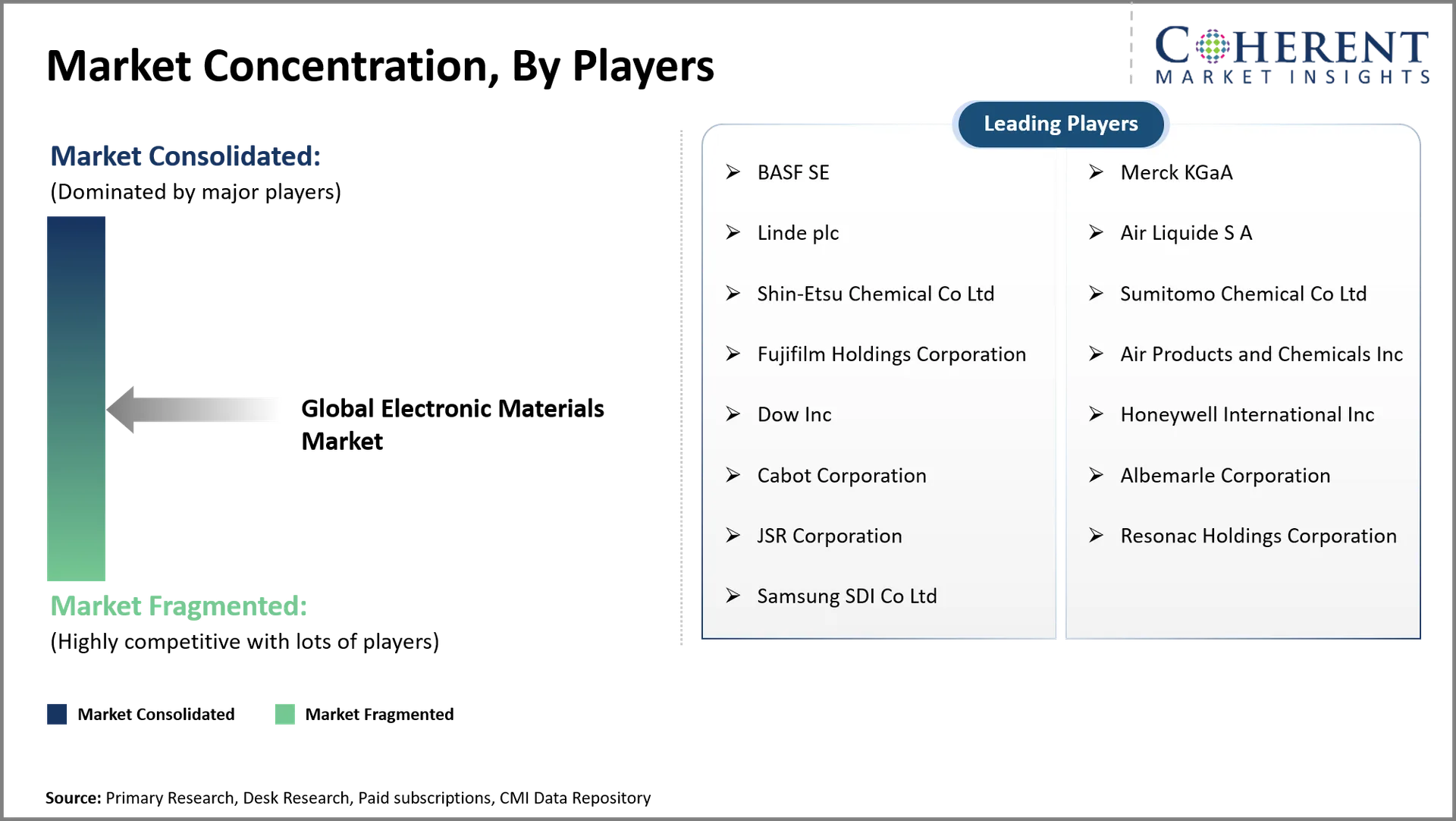
Companies covered: | BASF SE, Merck KGaA, Linde plc, Air Liquide S A, Shin-Etsu Chemical Co Ltd, Sumitomo Chemical Co Ltd, Fujifilm Holdings Corporation, Air Products and Chemicals Inc, Dow Inc, Honeywell International Inc, Cabot Corporation, Albemarle Corporation, JSR Corporation, Resonac Holdings Corporation, Samsung SDI Co Ltd | ||
Growth Drivers: |
| ||
Restraints & Challenges: |
| ||
Analyst Opinion (Expert Opinion)
- The future industry structure will increasingly center on materials engineered for advanced packaging and smaller semiconductor geometries. Heterogeneous integration will expand demand for interposers, low-loss dielectrics, bonding materials, and thermal solutions. Taiwan is developing certification platforms for these materials, strengthening supplier integration with chip manufacturers. Compound semiconductor materials will also be important for power electronics, optical systems and high frequency applications. Suppliers should focus on application specific formulations rather than wide commodity material catalogs.
- The strongest opportunities should emerge across advanced packaging materials, extreme ultraviolet photoresists, compound semiconductor substrates, and high-purity process chemicals. Artificial intelligence infrastructure creates particularly strong material requirements around high-bandwidth memory, advanced packaging, thermal management, and silicon photonics. Taiwan offers an important opportunity because its ecosystem connects materials development with foundries, packaging companies, and research institutions. The U.S. also has prospects for localized manufacture of high-purity chemicals and semiconductor grade polysilicon.
- Semiconductor customers demand uniform purity, process compatibility, defect control, and long-term supply reliability. Suppliers should form cooperative development programs with foundries, memory manufacturers and sophisticated packaging providers. The α-site concept in Taiwan offers a viable methodology to accelerate validation of materials with downstream customers. Companies should also diversify essential feedstocks and build out regional manufacturing capabilities. Local manufacturing offers reduced logistics vulnerability and improves adaptability to changes in client processes.
Speak to the analyst
Want personalized insights?
Take the findings above to one of our principal consultants, or have the report rebuilt around the segments, geographies and competitors you actually track.
Market Segmentation
- Product Insights (Revenue, USD Billion, 2021 - 2033)
- Solid
- Liquid
- Gas
- Application Insights (Revenue, USD Billion, 2021 - 2033)
- Silicon Wafers
- Printed Circuit Board Laminates
- Specialty Gases
- Wet Chemicals and Solvents
- Photoresists
- Others
- End User Insights (Revenue, USD Billion, 2021 - 2033)
- Semiconductors and Integrated Circuits
- Printed Circuit Boards
- Regional Insights (Revenue, USD Billion, 2021 - 2033)
- North America
- U.S.
- Canada
- Latin America
- Brazil
- Argentina
- Mexico
- Rest of Latin America
- Europe
- Germany
- U.K.
- Spain
- France
- Italy
- Russia
- Rest of Europe
- Asia Pacific
- China
- India
- Japan
- Australia
- South Korea
- ASEAN
- Rest of Asia Pacific
- Middle East
- GCC Countries
- Israel
- Rest of Middle East
- Africa
- South Africa
- North Africa
- Central Africa
- North America
Sources
Primary Research Interviews
- Electronic Materials Manufacturers & Suppliers
- Semiconductor Fabrication Companies
- Electronic Component Distributors & Traders
- ICIS Chemical Business Database
Magazines
- Electronic Design Magazine
- Semiconductor Digest
- Advanced Materials & Processes (ASM International)
- IEEE Spectrum
Journals
- Journal of Electronic Materials (Springer)
- Journal of Applied Physics (AIP Publishing)
- Microelectronics Engineering (Elsevier)
Associations
- SEMI (Semiconductor Equipment and Materials International)
- International Electronics Manufacturing Initiative (iNEMI)
- Electronic Components Industry Association (ECIA)
- American Chemical Society (ACS)
Public Domain Sources
- U.S. Geological Survey (USGS) – Critical Minerals & Materials Data
- World Trade Organization (WTO) – Trade Statistics
- U.S. International Trade Commission (USITC)
- European Chemicals Agency (ECHA)
Proprietary Elements
- CMI Data Analytics Tool
- Proprietary CMI Existing Repository of information for last 10 years
Get access to 250+ pages report
Every segment, forecast, competitor profile and data table behind the analysis above — available for instant download.
- ESOMAR Member
- ISO 9001:2015 Certified
- D-U-N-S Registered
- GDPR & CCPA Compliant
Frequently Asked Questions
The global electronic materials market is expected to stand at USD 83.50 Bn in 2026 and is expected to reach USD 127.30 Bn by 2033.
The CAGR of the global electronic materials market is projected to be 6.4% from 2026 to 2033.
Expanding semiconductor fabrication capacity and Rising artificial intelligence hardware production are the major factors driving the growth of the global electronic materials market.
High purity manufacturing complexity and Volatile raw material prices are the major factors hampering the growth of the global electronic materials market.
In terms of product, solid segment is estimated to dominate the market revenue share in 2026.
Electronic materials are specialized substances used to manufacture semiconductors, displays, circuit boards, sensors, and electronic components.
Artificial intelligence hardware requires advanced memory, packaging, thermal materials, substrates, and high-performance semiconductor materials.