

Global Interface IP Market Size and Forecast – 2026 To 2033
The global interface IP market is expected to grow from USD 2.50 Bn in 2026 to USD 5.95 Bn by 2033, registering a compound annual growth rate (CAGR) of 7% from 2026 to 2033. The global interface IP market is driven by increasing demand for high-bandwidth chip-to-chip connectivity. On March 31, 2025, Ayar Labs announced the industry’s first Universal Chiplet Interconnect Express (UCIe) optical interconnect chiplet to maximize AI infrastructure performance and efficiency while reducing latency and power consumption.
Key Takeaways of the Global Interface IP Market
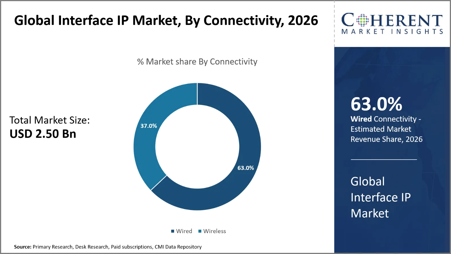
- The Wired segment is expected to account for 63.0% of the global interface IP market share in 2026. Expansion of chiplet-based semiconductor architectures is driving the growth of the segment. On September 23, 2026, Cadence announced an expanded partnership with TSMC to deliver advanced capabilities for AI and HPC designers.
- The High-Speed Interface IP segment is estimated to capture 55.0% of the market share in 2026. Increasing semiconductor design complexity is majorly driving the growth of the segment. On May 13, 2025, Siemens Digital Industries Software launched the Questa One verification portfolio. The platform incorporated artificial intelligence automation and predictive analytics for complex integrated circuit verification.
- The PCIe and CXL segment is estimated to capture 28.0% of the market share in 2026. Rising adoption of PCIe, CXL and advanced memory interfaces is majorly driving the growth of the segment. On June 16, 2025, Cadence announced an expansion of its collaboration with Samsung Foundry, including a new multi-year IP agreement to broaden Cadence memory and interface IP solutions in Samsung Foundry’s SF4X, SF5A and SF2P advanced process nodes.
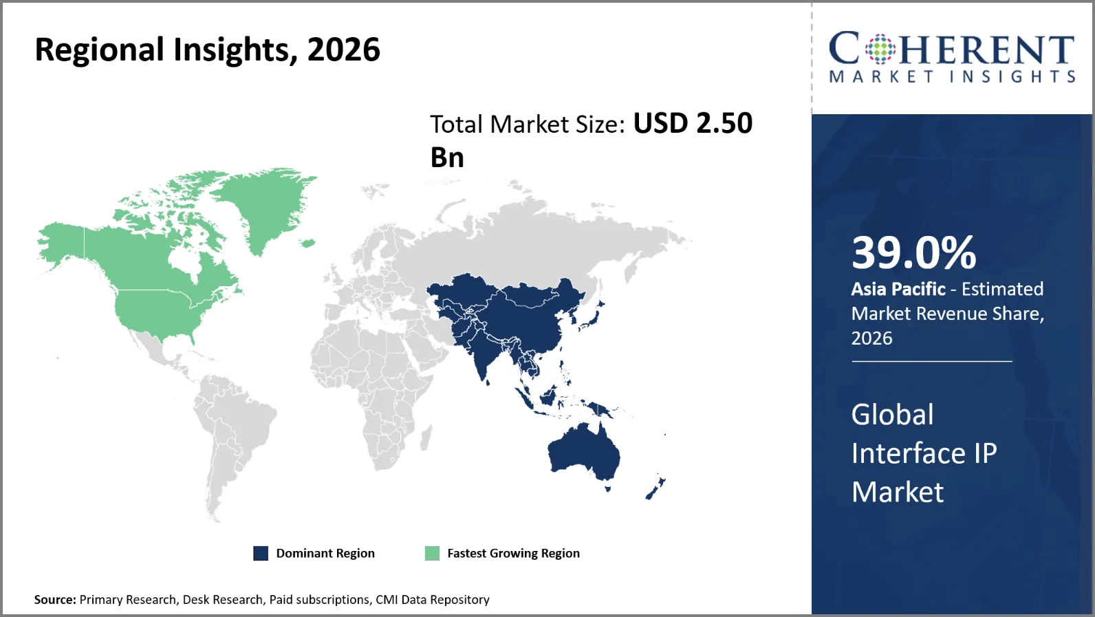
- Asia Pacific is expected to dominate the interface IP market in 2026 with a market share of 39.0%. Increasing integration of connectivity functions into advanced SoCs in Asia Pacific is driving the growth of the regional market. On June 1, 2026, MediaTek announced its role in enabling NVIDIA RTX Spark, introduced as a new class of processors powering Windows 11 PCs purpose-built for personal agents. It’s designed to build the future, unlock creative power, and run the latest games in slim laptops and small, ultra-efficient desktops.
- North America is expected to account for 31.0% share in 2026 and is projected to record the fastest growth over the forecast period. Expansion of automotive electronics and autonomous systems in North America is driving the growth of the regional market. On March 18, 2025, General Motors and NVIDIA announced they are collaborating on next-generation vehicles, factories and robots using AI, simulation, and accelerated computing.
Segmental Insights
Why Does Wired Dominate the Global Interface IP Market?
The wired segment is expected to account for 63.0% of the global interface IP market share in 2026. Semiconductor equipment require dependable, high bandwidth connectivity, which is why wired interface IP prevails. Wired interfaces have lower latency and better signal integrity than wireless options. They enable communication between processor, memory, storage, networking and peripheral devices across semiconductor architectures. Implementation of PCI Express and Compute Express Link standards requires customized interface IP. Wired interfaces also have mature specification, well established validation process and broad ecosystem compatibility. These characteristics reduce integration risks for application-specific integrated circuit and system-on-chip designers. Increasing artificial intelligence workloads further strengthen demand for high-bandwidth wired interconnects.
On August 26, 2025, Marvell Technology, Inc. announced the industry’s first 2nm 64 Gbps bi-directional die-to-die (D2D) interconnect, enabling chip designers to significantly boost the bandwidth and performance of next-generation XPUs. Delivering 32 Gbps of simultaneous two-way connectivity over a single wire, the interface IP sets a new standard for performance, power efficiency, and resiliency to meet the scaling demands of next-generation data centers.
- Current Industry Events of 2026
- Market Size Estimation
- Regional Breakdown
- Competitive Landscape
- Customer Intelligence
- Segmental Analysis
- Pricing Analysis
- Key Market Drivers, Challenges & Future Trends
- Customized Insights Section
Why is High-Speed Interface IP the Most Preferred Speed?
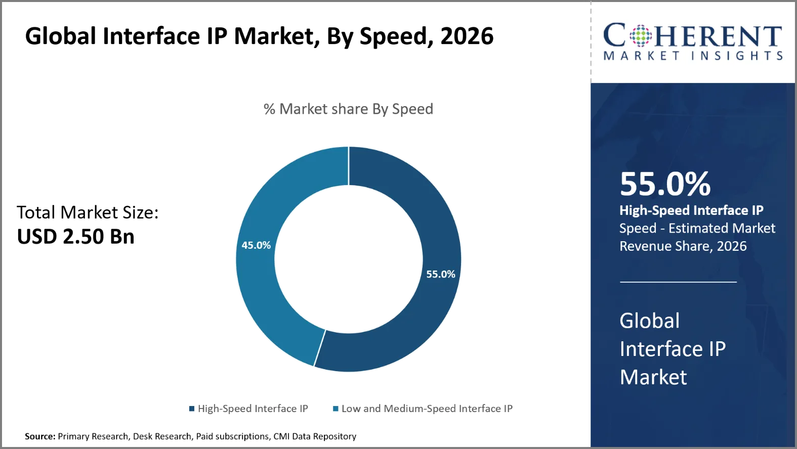
The high-speed interface IP segment is expected to account for 55.0% of the global interface IP market share in 2026. Modern CPUs handle ever increasing amounts of data. This means that high speed interface IP is preferred. AI accelerators require high speed connectivity with memory and other processing elements. High-speed interfaces reduce data-transfer bottlenecks between processors, accelerators, storage, and networking devices. They also improve system responsiveness without requiring proportional increases in physical interconnects. Advanced interface standards increasingly target higher transfer rates for data center and computing applications. Consequently, designers look for interface IP with larger bandwidth capability but at the same time preserve signal integrity. This requirement pushes semiconductor firms to provide verified high speed interface solutions. In February 2026, Global Unichip Corporation taped out UCIe 3.0 IP at 64 gigabits per second per lane. The implementation used TSMC N3P technology and CoWoS advanced packaging. It achieved 21 terabits per second per millimeter bandwidth density. The solution targets artificial intelligence, high-performance computing, data center, and networking applications.
PCIe and CXL Dominates the Global Interface IP Market
The PCIe and CXL segment is expected to account for 28.0% of the global interface IP market share in 2026. PCI express and Compute Express Link dominate as they address high-performance computing connectivity requirements. PCI Express provides standardized high-bandwidth connectivity for processors, accelerators, storage, and networking components. Compute Express Link extends high-speed connectivity toward coherent communication between processors and accelerators. Both standards benefit from strong industry adoption and established semiconductor development ecosystems. Artificial intelligence infrastructure is increasing requirements for accelerator connectivity and memory bandwidth. Compute Express Link is particularly relevant for memory expansion and heterogeneous computing architectures. PCI Express remains important across personal computers, servers, storage systems, and embedded platforms. Their complementary applications support sustained demand for related interface intellectual property. In April 2025, Rambus achieved Compute Express Link 2.0 compliance for its PCI Express 5.0 controller intellectual property. The controller supports 16 giga transfers per second across an eight-lane configuration. The compliance demonstrates readiness for coherent memory and accelerator connectivity. This development will allow more use of PCI Express and Compute Express Link in data center architecture.
Current Events and their Impact
Current Events | Description and its Impact |
European Union Cyber Resilience Act, Regulation (EU) 2024/2847 |
|
European Chips Act, Regulation (EU) 2023/1781 |
|
Interface IP Market Dynamics
Market Drivers
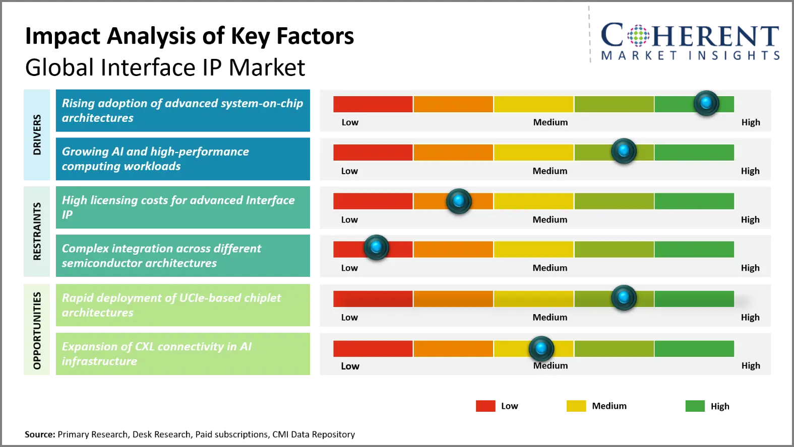
Rising adoption of advanced system-on-chip architectures
Advanced system-on-chip architectures are slowly combining processors, accelerators, memory controllers, and connection functions. This combination drives a demand for reliable interface intellectual property blocks. Increasingly sophisticated chips require designers to connect various functional components using reusable interface IP. High-speed interfaces provide communications between the CPU cores, memory subsystems, storage controllers and external devices. Standardized interface protocols can also simplify integration and reduce development complexity. Growing chip functionality therefore supports demand for flexible and scalable interface IP solutions.
On April 22, 2025, Intel unveiled the second-generation Intel AI-enhanced software-defined vehicle (SDV) system-on-chip (SoC), the automotive industry’s first multi-process node chiplet architecture. Engineered to meet the growing demands of intelligent, connected vehicles, the new SoC provides automakers scalable performance, advanced AI capabilities and optimized cost efficiency.
Growing AI and high-performance computing workloads
AI and high-performance computing workloads require ever faster data transfer across processors, accelerators, memory, and storage. High-bandwidth interface IP helps alleviate communication constraints in these computing systems. Graphics processing units and artificial intelligence accelerators increasingly require fast connections for handling large datasets. Advanced interfaces also support coherent communication between processors and memory resources. Data center operators therefore require semiconductor platforms capable of sustaining intensive computational workloads. This demand supports adoption of high-speed interface IP across advanced computing architectures.
On May 31, 2026, NVIDIA announced that the world’s technology leaders are planning to adopt NVIDIA Vera, the first CPU built for AI agents. Now in full production, NVIDIA Vera is a new class of processor enabling 1.8x faster task completion compared with x86 CPUs to drive diverse workloads across industries, including agentic AI, reinforcement learning and data processing, generating more data center token revenue.
Emerging Trends
- Expansion of PCI Express 6.0 and 7.0 Interfaces: Interface IP developers increasingly support newer PCI Express generations with higher data rates. These standards address bandwidth requirements across artificial intelligence accelerators, servers, storage systems, and high-performance computing platforms requiring faster device-to-device communication.
- Growing Adoption of Compute Express Link: Compute Express Link is being adopted in accelerator-rich next generation computing architectures and memory expansion systems. Interface IP suppliers have developed solutions for coherent connectivity for artificial intelligence and data-intensive workloads that progressively include processors, accelerators and memory resources.
- Integration of Chiplet-Based Architectures: Chiplet architectures are also driving the need for standardized die-to-die interface IPs to enable modular semiconductor designs. New technologies such as Universal Chiplet Interconnect Express allow independently designed chiplets to talk to one another, boosting design flexibility and permitting ever more sophisticated CPU architectures.
- Increasing Focus on Secure Interface IP: Interface IP security features are being taken more seriously by semiconductor designers. As data moves across processors, accelerators, memory, and linked devices, hardware-based protection, authentication, encryption support, and integrity monitoring become more important.
Regional Insights
Why is Asia Pacific a Strong Market for Interface IP?
Asia Pacific is expected to account for a market share of 39.0% in 2026. Artificial intelligence infrastructure and improved semiconductor manufacturing drive the growth of interface IP use in Asia Pacific. The area has important chipmaking hubs in Taiwan, South Korea, Japan and China. TSMC's Open Innovation Platform supports PCI Express, Compute Express Link, Ethernet, and Universal Chiplet Interconnect Express technologies. Its ecosystem includes silicon-verified and production-proven intellectual property. TSMC also expanded CoWoS packaging capabilities for artificial intelligence processors requiring high-bandwidth memory connections. These developments increase demand for high-speed physical-layer, controller, and die-to-die interface IP. The region's distinct strength comes from close integration between foundries, semiconductor designers, packaging providers, and intellectual property developers.
Why Does North America Interface IP Market Exhibit High Growth?
North America is expected to register the fastest growth with a CAGR of 8.0% over the forecast period. North America is projected to account for 31.0% of the global interface IP market in 2026. North America is expanding interface IP adoption through hyperscale computing and custom artificial intelligence silicon development. The major cloud firms are rapidly building customized CPUs that require PCI Express, Ethernet, Compute Express Link, and memory interfaces. By 2025, Synopsys will have powered more than 3,800 customer tapeouts across seven generations of PCI Express. Rambus has developed PCI Express 6.0 interface technology supporting Compute Express Link 3.0 for artificial intelligence systems. These developments increase requirements for validated physical-layer and controller IP. Chiplet-based processor designs are also creating additional requirements for standardized die-to-die connectivity. North America's distinct growth factor is its concentration of hyper scalers, custom silicon developers, electronic design automation companies, and semiconductor IP suppliers.
Global Interface IP Market Outlook for Key Countries
Why is China Emerging as a Major Hub in the Interface IP Market?
China is building interface IP demand through domestic semiconductor design and technology localization projects. Chinese fabless businesses are increasingly developing CPUs, artificial intelligence accelerators, networking chips and system-on-chip platforms. These products require reusable interface bricks for memory, storage, networking and peripheral connectivity. Among the economies, China also has one of the largest semiconductor wafer manufacturing capacities. Demand for high-speed accelerator and memory connectivity is heating up as the country’s artificial intelligence infrastructure grows. Domestic processor development is also driving more reliance on design resources under local control. This opens up potential for interface IP to support customized architectures and homegrown semiconductor platforms. The rising emphasis on semiconductor technology independence and regional design capabilities is a unique growth driver for China.
Is U.S. the Next Growth Engine for the Interface IP Market?
The U.S. is driving demand for interface IP for AI accelerators, hyperscale data centers, and the creation of specialized processors. Cloud firms are building more specialized silicon that needs high-speed communication between CPUs, accelerators, memory and networking components. Synopsys said it has more than 3,800 customer tapeouts across seven PCI Express generations by 2025. Advanced accelerator architectures also require high-bandwidth connections for large-scale artificial intelligence workloads. The U.S. hosts major semiconductor IP and electronic design automation developers supporting complex system-on-chip development. Domestic semiconductor manufacturing investments are additionally strengthening demand for qualified interface IP. The country's distinct growth factor is the rapid development of hyperscale computing platforms and custom artificial intelligence processors.
Taiwan Interface IP Market Analysis and Trends
Taiwan is seeing growth in interface IP activities with advanced foundry manufacturing and chiplet-based semiconductor development. TSMC’s Open Innovation Platform delivers third-party IP that has been silicon-verified and production-proven. Its supported technologies include PCI Express 1.0 through 6.0, Compute Express Link 3.0, and 400G and 800G Ethernet. TSMC also supports Universal Chiplet Interconnect Express technology for superior multi-die architecture. Its innovative packaging portfolio includes CoWoS technologies for high-performance computing (HPC) applications. These developments require more advanced die-to-die, memory, and high-speed connection systems. The unique development driver for Taiwan is the tight integration of advanced foundries, IP vendors, semiconductor designers and advanced packaging providers.
Japan Interface IP Market Analysis and Trends
Interface IP demand is being driven by data center infrastructure, automotive computing and innovative semiconductor technologies in Japan. Renesas Electronics is working on solutions for cloud and data center applications employing PCI Express buffers and DDR5 memory interfaces. It highlighted next-generation data center networking at 102.4 terabits per second in its 2025 technology presentation. Japanese semiconductor businesses also make automobile processors that require dependable communication between processors, sensors, memory and network components. High-speed automobile interfaces are further stressed by advanced driver assistance systems. Japan’s deeply rooted automotive electronics ecosystem provides a unique source of need for robust interface technology. Its separate growth factor is the convergence of automotive computing requirements with expanding data center infrastructure.
South Korea Interface IP Market Analysis and Trends
South Korea is increasing interface IP requirements through high-bandwidth memory and Compute Express Link development. Samsung Electronics developed a 128-gigabyte CXL 2.0 DRAM supporting PCI Express 5.0 and eight lanes. The product provides bandwidth of up to 35 gigabytes per second and supports memory pooling. Samsung also established CXL infrastructure certified by Red Hat for complete server validation. SK hynix identifies Compute Express Link as an important technology connecting processors, graphics processors, memory, and computing components. These advances create requirements for CXL, PCI Express and memory-interface IP. What makes South Korea unique as a development driver is the quick combination of high-bandwidth memory technology with AI computer architecture.
Global Interface IP Market - Chiplet Architectures and Heterogeneous Computing Adoption by Region/Country:
Region/Country | Adoption Indicators 2025-2026 | Key Market Players | Advanced Packaging Focus |
North America | Strong deployment of UCIe, chiplets, and heterogeneous computing for artificial intelligence | Intel, AMD, NVIDIA, Synopsys, Cadence, Ayar Labs | 2.5D |
Asia Pacific | Rapid expansion of chiplet manufacturing, foundry integration, and UCIe development | TSMC, Samsung Electronics, SK hynix, Global Unichip Corporation, Socionext | 3D |
Europe | Growing adoption through automotive, industrial, research, and semiconductor design ecosystems | Siemens, Arm, Infineon Technologies, STMicroelectronics | Advanced system-in-package |
China | Increasing development of domestic chiplet architectures and heterogeneous processors | Semiconductor Manufacturing International Corporation, Huawei, JCET, Tongfu Microelectronics | CoWoS |
Japan | Expanding chiplet development across automotive, computing, memory, and semiconductor equipment | Renesas Electronics, Sony Semiconductor Solutions, Socionext, Kioxia | SoIC |
South Korea | Strong integration of chiplets with high-bandwidth memory and advanced semiconductor packaging | Samsung Electronics, SK hynix, Rebellions | Hybrid bonding |
Taiwan | Extensive foundry and advanced packaging infrastructure supports multi-die integration | Taiwan Semiconductor Manufacturing Company, Global Unichip Corporation, ASE Technology | HBM integration |
How is Rapid Deployment of UCIe-Based Chiplet Architectures Creating New Growth Opportunities in the Interface IP Market?
The rapid deployment of UCIe designs is creating new opportunities for interface IP suppliers by establishing a standard for communication across separately produced chiplets. The Universal Chiplet Interconnect Express spec provides die-to-die connections for diverse chiplet functions and manufacturers. UCIe 2.0 added management, testing and 3D packaging capability, raising requirements beyond basic die-to-die connection. UCIe 3.0 boosted data rates to 64 mega transfers per second, aiming to provide more capacity for artificial intelligence and high-performance computing applications. Intel, Advanced Micro Devices, Arm, Samsung Electronics, TSMC, and Synopsys are among organizations participating in the UCIe ecosystem. These developments create demand for PHY, controller, verification, compliance, and advanced packaging interface IP. In August 2026, Intel highlighted early UCIe adoption across its next-generation processor architectures. Diamond Rapids combines UCIe-S interconnects with advanced packaging and high-bandwidth memory. Wildcat Lake also introduces UCIe connectivity in an Intel processor for mainstream artificial intelligence platforms.
Market Players, Key Development, and Competitive Landscape
Key Developments
- On September 1, 2026, Cadence announced that its PHY and controller IP for the PCI Express (PCIe) 6.0 specification, implemented in the TSMC N3 process, achieved first-pass success at the recent PCI-SIG compliance workshop. The complete Cadence subsystem solution, comprising both PHY and controller, successfully passed all official PCIe 6.0 compliance specification tests and is on PCI-SIG’s Integrators List.
- On September 9, 2024, Synopsys, Inc. announced the industry's first complete UCIe IP solution operating at up to 40 Gbps per pin to address the increased compute performance requirements of the world's fastest AI data centers. The UCIe interconnect is critical for high-bandwidth, low-latency die-to-die connectivity in multi-die packages, enabling more data to travel efficiently across heterogeneous and homogeneous dies, or chiplets, in today's AI data center systems.
- On June 12, 2024, Rambus announced the launch of its PCI Express (PCIe) 7.0 IP portfolio, encompassing a comprehensive suite of IP solutions. The PCIe 7.0 Controller designed to deliver the high bandwidth, low latency, and robust performance required for next-generation AI and HPC applications.
Competitive Landscape
Leading interface IP players are moving from discrete protocol blocks to full connectivity subsystems. Synopsys is broadening its portfolio in PCI Express, Compute Express Link, Universal Chiplet Interconnect Express and high-speed SerDes. Its UCIe IP includes controller, PHY, adaptor and verification IP to enable multi-die designs. Cadence is investing in proven connection silicon for AI and high-speed computing. It achieved first-pass certification for its PCI Express 6.0 subsystem on TSMC N3 technology in 2026. Cadence also expanded UCIe 64G, PCI Express 7.0, and 224G SerDes offerings with Samsung Foundry. These strategies show increasing competition around protocol coverage, process-node qualification, interoperability, and complete subsystem integration.
Market Report Scope
Report Coverage | Details | ||
Base Year | 2025 | Market Size in 2026: | USD 2.50 Bn |
Historical Data For: | 2020 To 2024 | Forecast Period: | 2026 To 2033 |
Forecast Period 2026 To 2033 CAGR: | 7% | 2033 Value Projection: | USD 5.95 Bn |
Geographies covered: |
| ||
Segments covered: |
| ||
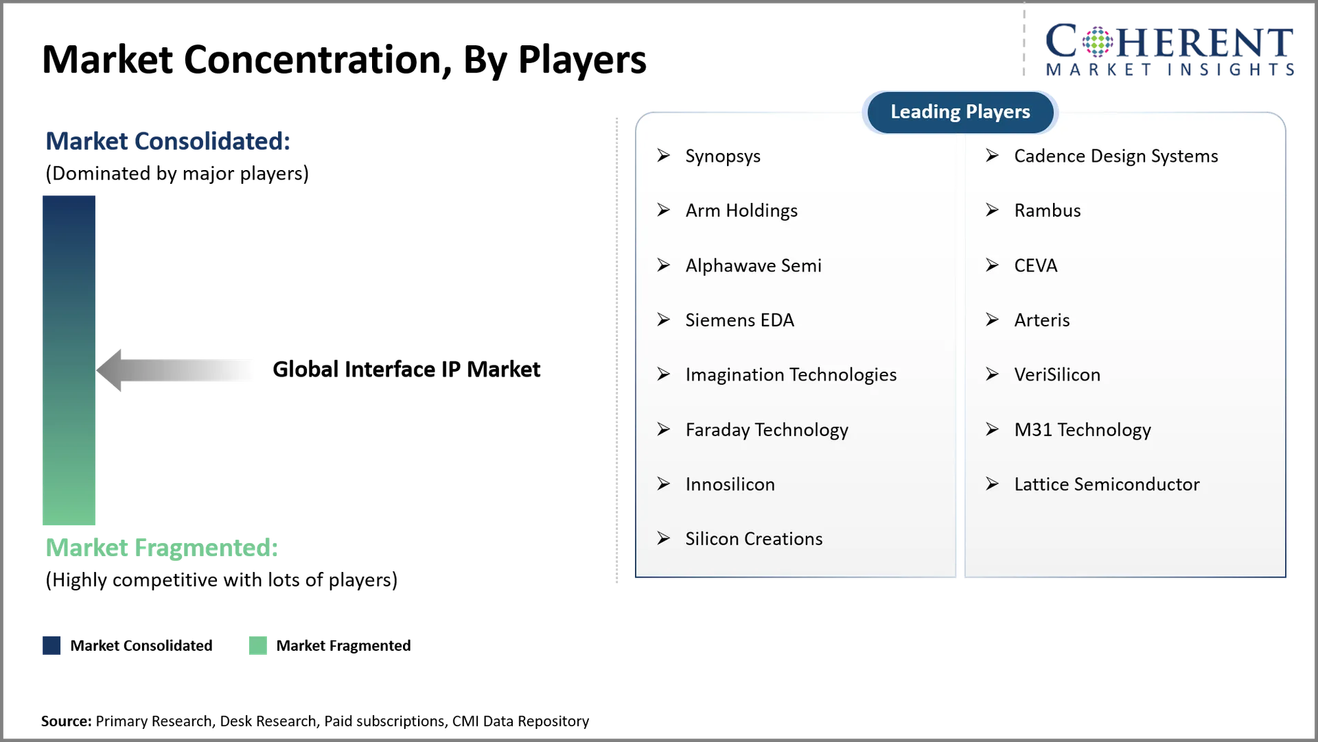
Companies covered: | Synopsys, Cadence Design Systems, Arm Holdings, Rambus, Alphawave Semi, CEVA, Siemens EDA, Arteris, Imagination Technologies, VeriSilicon, Faraday Technology, M31 Technology, Innosilicon, Lattice Semiconductor, Silicon Creations | ||
Growth Drivers: |
| ||
Restraints & Challenges: |
| ||
Analyst Opinion (Expert Opinion)
- Interface IP development is expected to shift increasingly toward multi-die connectivity and heterogeneous computing architectures. PCI Express and Compute Express Link should remain important for accelerator, memory, storage, and processor connectivity. Universal Chiplet Interconnect Express should create a separate growth path as chiplet integration expands. Synopsys already supports UCIe connections across AXI, CXS, CHI C2C, PCI Express, and Compute Express Link. Cadence is developing UCIe solutions across standard and advanced packaging technologies.
- The strongest opportunity should center on UCIe, PCI Express 7.0, CXL 4.0, and advanced SerDes IP. Artificial intelligence accelerators will require connectivity supporting increasing bandwidth across compute, memory, and storage components. CXL 4.0 supports 128 GT/s and expands memory pooling and accelerator connectivity capabilities. The U.S. and Taiwan should remain important focus countries because their ecosystems combine advanced chip design and manufacturing capabilities. South Korea also offers substantial opportunities through memory-centric computing and advanced foundry development.
- Players seeking an edge should prioritize silicon-proven IP across leading process nodes and advanced packaging platforms. Supporting multiple protocols through common PHY architectures can reduce integration complexity for customers. Another significant aspect for comapnies is to invest substantially in verification IP. Interoperability is more difficult with greater signaling speeds. Cadence’s attainment of PCI Express 6.0 certification highlights the value of rigorous interoperability validation. Synopsys's complete UCIe portfolio similarly demonstrates the value of combining PHY, controller, verification, and package-level capabilities.
Speak to the analyst
Want personalized insights?
Take the findings above to one of our principal consultants, or have the report rebuilt around the segments, geographies and competitors you actually track.
Market Segmentation
- Connectivity Insights (Revenue, USD Billion, 2021 - 2033)
- Wired
- Wireless
- Speed Insights (Revenue, USD Billion, 2021 - 2033)
- High-Speed Interface IP
- Low and Medium-Speed Interface IP
- Interface Type Insights (Revenue, USD Billion, 2021 - 2033)
- PCIe and CXL
- UCIe and Die-to-Die
- USB and Ethernet
- DDR and LPDDR
- HBM
- MIPI and Display Interface
- Others
- Application Insights (Revenue, USD Billion, 2021 - 2033)
- Data Centers and AI Computing
- Consumer Electronics
- Automotive Electronics
- Industrial and Internet of Things
- Telecommunications
- Aerospace and Defense
- Regional Insights (Revenue, USD Billion, 2021 - 2033)
- North America
- U.S.
- Canada
- Latin America
- Brazil
- Argentina
- Mexico
- Rest of Latin America
- Europe
- Germany
- U.K.
- Spain
- France
- Italy
- Russia
- Rest of Europe
- Asia Pacific
- China
- India
- Japan
- Australia
- South Korea
- ASEAN
- Rest of Asia Pacific
- Middle East
- GCC Countries
- Israel
- Rest of Middle East
- Africa
- South Africa
- North Africa
- Central Africa
- North America
- Key Players Insights
- Synopsys
- Cadence Design Systems
- Arm Holdings
- Rambus
- Alphawave Semi
- CEVA
- Siemens EDA
- Arteris
- Imagination Technologies
- VeriSilicon
- Faraday Technology
- M31 Technology
- Innosilicon
- Lattice Semiconductor
- Silicon Creations
Sources
Primary Research Interviews
- Semiconductor IP Providers & Licensors
- Fabless Semiconductor Companies
- Electronic Design Automation (EDA) Tool Vendors
- System-on-Chip (SoC) Design Engineers & Architects
Magazines
- IEEE Spectrum Magazine
- Electronic Design Magazine
- EE Times Magazine
- Semiconductor Engineering Magazine
Journals
- IEEE Journal of Solid-State Circuits
- ACM Transactions on Design Automation of Electronic Systems
- Journal of Semiconductor Technology and Science
Associations
- SEMI (Semiconductor Equipment and Materials International)
- IP Europe (Intellectual Property Industry Association)
- Global Semiconductor Alliance (GSA)
- Electronic Components Industry Association (ECIA)
Public Domain Sources
- U.S. Patent and Trademark Office (USPTO) – IP Filings & Records
- World Intellectual Property Organization (WIPO) Database
- European Semiconductor Industry Association (ESIA) Public Reports
- U.S. International Trade Commission (USITC) Reports
Proprietary Elements
- CMI Data Analytics Tool
- Proprietary CMI Existing Repository of Information for the last 10 years
Get access to 250+ pages report
Every segment, forecast, competitor profile and data table behind the analysis above — available for instant download.
- ESOMAR Member
- ISO 9001:2015 Certified
- D-U-N-S Registered
- GDPR & CCPA Compliant
Frequently Asked Questions
The global interface IP market is expected to stand at USD 2.50 Bn in 2026 and is expected to reach USD 5.95 Bn by 2033.
The CAGR of the global interface IP market is projected to be 7% from 2026 to 2033.
Rising adoption of advanced system-on-chip architectures and Growing AI and high-performance computing workloads are the major factors driving the growth of the global interface IP market.
High licensing costs for advanced Interface IP and Complex integration across different semiconductor architectures are the major factors hampering the growth of the global interface IP market.
In terms of connectivity, wired segment is estimated to dominate the market revenue share in 2026.
Interface IP is reusable semiconductor intellectual property that enables communication between processors, memory, storage, peripherals, and other components.
Chiplet architectures increase demand for validated die-to-die controllers, physical layers, and interoperability solutions.