

Global Semiconductor Etching Equipment Market Size and Forecast – 2026 To 2033
The global semiconductor etching equipment market is expected to grow from USD 18.00 Bn in 2026 to USD 32.00 Bn by 2033, registering a compound annual growth rate (CAGR) of 9% from 2026 to 2033. The global semiconductor etching equipment market is driven by growing demand for artificial intelligence processors. On June 12, 2025, AMD launched the AMD Instinct MI350 Series, delivering up to 4x generation-on-generation AI compute improvement and up to 35x leap in inferencing performance.
Key Takeaways of the Global Semiconductor Etching Equipment Market
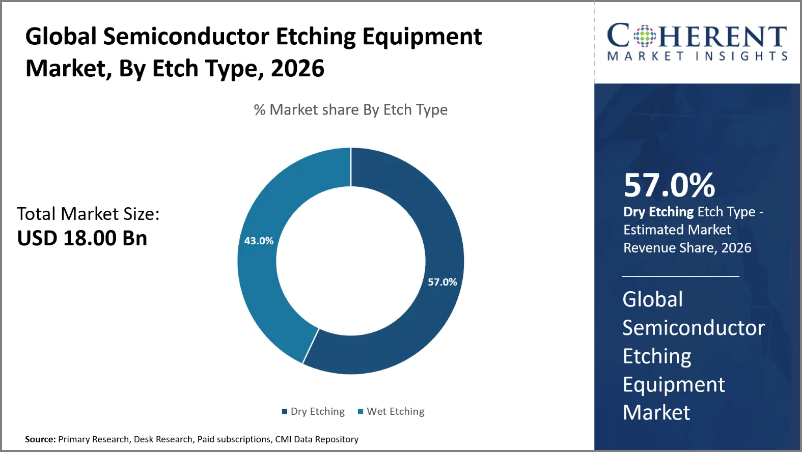
- The Dry Etching segment is expected to account for 57.0% of the global semiconductor etching equipment market share in 2026. Rising memory semiconductor production is driving the growth of the segment. On June 18, 2026, SK hynix shipped 12-layer HBM4 samples to major customers. The HBM4 uses increasingly complex stacked memory structures.
- The 3D segment is estimated to capture 55.0% of the market share in 2026. Increasing complexity of advanced technology nodes is majorly driving the growth of the segment. On June 16, 2025, Tokyo Electron and imec extended their partnership for another five years. Their program targets advanced logic, future memory, 3D integration and nodes beyond 2 nanometers.
- The Logic and Memory segment is estimated to capture 79.0% of the market share in 2026. Expansion of electric vehicle semiconductor applications is majorly driving the growth of the segment. On May 19, 2025, Infineon announced power module supplies for Rivian's R2 electric vehicle platform. The platform will use silicon carbide and silicon modules for traction inverters.
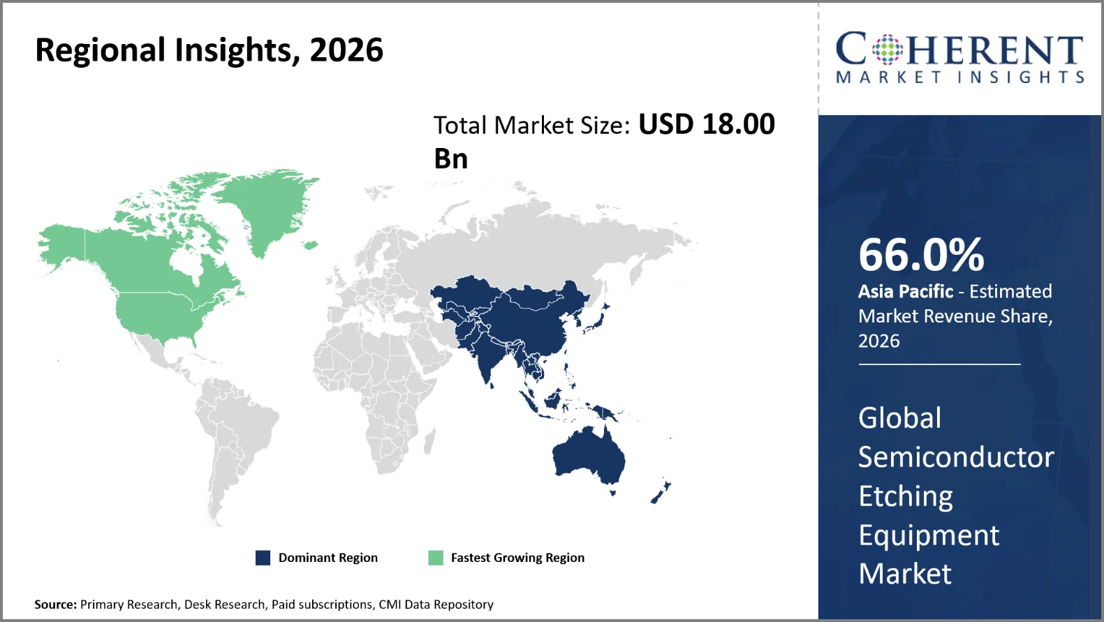
- Asia Pacific is expected to dominate the semiconductor etching equipment market in 2026 with a market share of 66.0%. Growing demand for high aspect ratio etching in Asia Pacific is driving the growth of the regional market. On August 30, 2026, Samsung Electronics presented its V10 V-NAND technology with more than 400-word lines. The company developed advanced three-stack high-aspect-ratio contact merging technology.
- North America is expected to account for 19.0% share in 2026 and is projected to record the fastest growth over the forecast period. Rising semiconductor capital expenditure in North America is driving the growth of the regional market. On June 18, 2025, Texas Instruments (TI) announced its plans to invest more than USD 60 billion across seven U.S. semiconductor fabs, making this the largest investment in foundational semiconductor manufacturing in U.S. history.
Segmental Insights
Why Does Dry Etching Dominate the Global Semiconductor Etching Equipment Market?
The dry etching segment is expected to account for 57.0% of the global semiconductor etching equipment market share in 2026. Dry etching dominates because advanced semiconductor fabrication requires precise, directional material removal. Plasma-based processes create highly anisotropic profiles across extremely small device structures. This precision supports advanced transistor architectures, multilayer interconnects, and high-density memory cells. Dry etching also provides stronger control over selectivity and critical dimensions. Manufacturers increasingly require consistent wafer-level uniformity across increasingly complex process layers. These requirements make dry etching essential for advanced logic, dynamic random-access memory, and three-dimensional NAND production.
On February 10, 2026, Applied Materials, Inc. introduced new deposition, etch and materials modification systems that boost the performance of leading-edge logic chips at 2nm and beyond. The technologies supercharge AI compute through atomic-scale improvements to the most fundamental electronic building block, the transistor.
- Current Industry Events of 2026
- Market Size Estimation
- Regional Breakdown
- Competitive Landscape
- Customer Intelligence
- Segmental Analysis
- Pricing Analysis
- Key Market Drivers, Challenges & Future Trends
- Customized Insights Section
Why is 3D the Most Crucial Dimension?
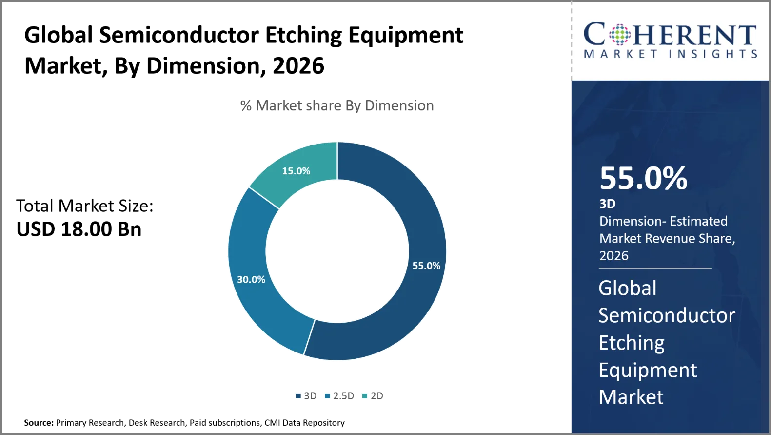
The 3D segment is expected to account for 55.0% of the global semiconductor etching equipment market share in 2026. 3D device structures are increasingly important because semiconductor scaling now depends on vertical integration. Traditional planar scaling faces physical limitations involving leakage, performance, and available surface area. Three-dimensional architectures increase transistor density without relying exclusively on smaller lateral dimensions. Gate-All-Around transistors require sophisticated etching around vertically structured semiconductor channels. Three-dimensional NAND requires deep, uniform channels across hundreds of stacked memory layers. These structures create significantly greater etching complexity than conventional planar devices.
On April 23, 2026, TSMC debuted its latest innovation in its most advanced process technology at the Company’s 2026 North America Technology Symposium. TSMC’s new A13 process is a direct shrink of its industry-leading A14 node announced in 2025, enabling even more compact and efficient designs to address insatiable customer demand in computational requirements for next-generation artificial intelligence, high-performance computing (HPC), and mobile applications.
Logic and Memory Dominates the Global Semiconductor Etching Equipment Market
The logic and memory segment is expected to account for 79.0% of the global semiconductor etching equipment market share in 2026. Logic and memory manufacturing dominate because both technologies require extensive pattern transfer across numerous device layers. Advanced logic devices contain complex transistor structures, contacts, spacers, and interconnect features. Memory devices require repeated etching processes across densely stacked structures. Three-dimensional NAND manufacturing particularly increases demand for deep and high-aspect-ratio etching. Dynamic random-access memory manufacturing also requires precise pattern definition across increasingly compact cells. Logic manufacturing benefits from advanced Gate-All-Around architectures and complementary field-effect transistor development.
On February 25, 2025, Micron Technology, Inc. announced it is the first in the industry to ship samples of its 1γ (1-gamma), sixth-generation (10nm-class) DRAM node-based DDR5 memory designed for next-generation CPUs to ecosystem partners and select customers. This 1γ DRAM milestone builds on Micron’s previous 1α (1-alpha) and 1β (1-beta) DRAM node leadership to deliver innovations that will power future computing platforms from the cloud to industrial and consumer applications to Edge AI devices like AI PCs, smartphones and automobiles.
Current Events and their Impact
Current Events | Description and its Impact |
U.S. - Semiconductor Manufacturing Equipment Export Controls |
|
Japan Foreign Exchange And Foreign Trade Act Export Controls |
|
Semiconductor Etching Equipment Market Dynamics
Market Drivers
Expansion of advanced semiconductor fabrication plants
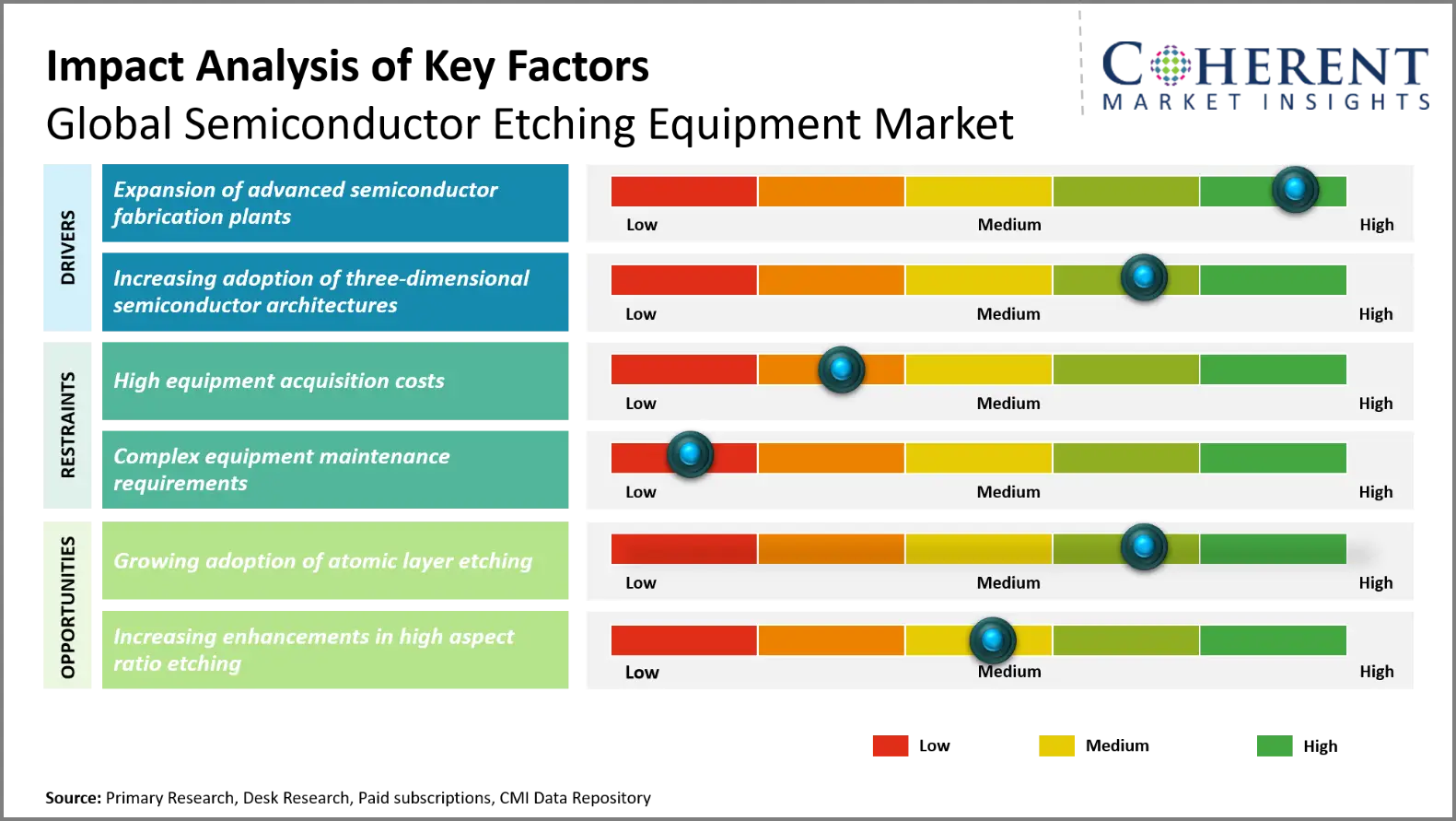
The expansion of advanced semiconductor fabrication plants is increasing demand for sophisticated etching equipment. New fabs require equipment supporting smaller process nodes and increasingly complex wafer structures. Leading manufacturers are investing heavily in advanced logic, memory, and specialty semiconductor production facilities. These facilities require precise plasma control, high wafer uniformity, and consistent critical-dimension management. Etching equipment becomes especially important as fabrication processes add more pattern-transfer steps. New fabrication capacity across Taiwan, South Korea, China, Japan, the United States, and Europe strengthens equipment demand. Government semiconductor incentives are also accelerating domestic fab construction and equipment procurement.
On May 8, 2025, Infineon Technologies AG announced it has received final approval for the funding of its new plant in Dresden (Smart Power Fab) from the German Federal Ministry for Economic Affairs. Infineon is expanding the site in order to meet customer demand for example for renewable energies, efficient data centers and electromobility. Infineon will invest USD 5.60 billion, creating as many as 1,000 new jobs.
Increasing adoption of three-dimensional semiconductor architectures
The increasing adoption of three-dimensional semiconductor architectures is raising the technical requirements for semiconductor etching equipment. Modern devices increasingly use vertically structured transistors and multilayer memory architectures. Gate-All-Around transistor designs require highly selective etching around vertically arranged semiconductor channels. Three-dimensional NAND requires extremely deep and uniform etching through stacked material layers. These structures demand exceptional aspect-ratio control, selectivity, profile uniformity, and minimal structural damage. Atomic layer etching can provide greater material-removal control for sensitive three-dimensional structures.
On January 30, 2025, Intel revealed this month that the Intel 18A process technology is progressing toward high-volume production in the second half of 2025. Intel 18A brings foundry customers to the forefront of innovation, introducing two semiconductor manufacturing breakthroughs to improve Intel products and those of Intel Foundry customers.
Emerging Trends
- Rising Adoption of Atomic Layer Etching: Atomic layer etching is gaining importance for advanced semiconductor structures requiring exceptional dimensional control. The technology removes material in highly controlled cycles. It supports selective processing for Gate-All-Around transistors and increasingly complex three-dimensional memory architectures.
- Growing Demand for High-Aspect-Ratio Etching: Three-dimensional NAND and advanced logic devices require increasingly deeper structures. Equipment manufacturers are developing plasma processes supporting greater aspect ratios while maintaining profile uniformity. These capabilities improve channel formation and reduce defects across vertically stacked semiconductor structures.
- Integration Of Artificial Intelligence into Etch Process Control: Semiconductor manufacturers are increasingly applying artificial intelligence to equipment monitoring and process optimization. Advanced analytics can identify process drift and equipment anomalies earlier. This approach improves yield consistency while reducing unplanned equipment downtime during high-volume manufacturing.
- Development Of Lower-Impact Etching Processes: Environmental requirements are encouraging equipment manufacturers to reduce process emissions and chemical consumption. New plasma chemistries and chamber designs target lower environmental impact. These developments can reduce resource consumption while maintaining etch performance for advanced semiconductor manufacturing processes.
Regional Insights
Why is Asia Pacific a Strong Market for Semiconductor Etching Equipment?
Asia Pacific is expected to account for a market share of 66.0% in 2026. Asia Pacific remains the central production base for advanced semiconductor fabrication and etching equipment demand. China, Taiwan, South Korea, and Japan collectively accounted for most global equipment spending in 2025. Taiwan and South Korea recorded particularly strong equipment growth from artificial intelligence semiconductor investments. China maintained substantial fabrication expansion across mature and selected advanced nodes. Japan recorded 22% equipment spending growth, supported by domestic advanced-node manufacturing. The region also benefits from concentrated suppliers, including Tokyo Electron and other Japanese equipment companies. Increasing high-bandwidth memory production and advanced packaging further strengthen regional etching requirements.
Why Does North America Semiconductor Etching Equipment Market Exhibit High Growth?
North America is expected to register the fastest growth with a CAGR of 9.8% over the forecast period. North America is projected to account for 19.0% of the global semiconductor etching equipment market in 2026. North American growth is increasingly linked to domestic fabrication expansion and advanced semiconductor localization. TSMC Arizona began 4-nanometer volume production during the fourth quarter of 2024. Its second Arizona facility is being equipped for 3-nanometer production. TSMC also announced three additional U.S. fabrication plants and two advanced packaging facilities. Intel continues developing advanced process manufacturing capabilities in Arizona and Ohio. These projects require sophisticated etching systems for logic, interconnect, and transistor fabrication.
Global Semiconductor Etching Equipment Market Outlook for Key Countries
Why is China Emerging as a Major Hub in the Semiconductor Etching Equipment Market?
China remains the largest national destination for semiconductor manufacturing equipment. Domestic manufacturers continued investing heavily in mature-node capacity and selected advanced technologies during 2025. Chinese companies are also increasing domestic equipment development amid technology restrictions. Semiconductor Manufacturing International Corporation and Hua Hong Semiconductor remain important domestic fabrication participants. Local equipment companies are developing etching platforms for logic, memory, power, and specialty devices. Strong government support for semiconductor self-sufficiency continues encouraging domestic equipment procurement. These conditions sustain substantial demand for etching systems despite tighter international technology controls
Is U.S. the Next Growth Engine for the Semiconductor Etching Equipment Market?
The U.S. market is expanding through government-supported semiconductor manufacturing localization. TSMC Arizona produced 4-nanometer chips during 2024 and is preparing 3-nanometer manufacturing. The company announced plans involving three additional fabrication plants and two advanced packaging facilities. Intel is also advancing domestic leading-edge process development and manufacturing. Lam Research and Applied Materials provide major domestic expertise in plasma etching technologies. Increasing domestic artificial intelligence processor production is raising requirements for advanced transistor and interconnect etching. Semiconductor equipment localization is therefore becoming an important structural growth factor.
Taiwan Semiconductor Etching Equipment Market Analysis and Trends
Taiwan is experiencing strong etching equipment demand from leading-edge logic and artificial intelligence computing. Taiwan Semiconductor Manufacturing Company is preparing multiple 2-nanometer fabrication phases across Hsinchu and Kaohsiung. The company reported that advanced technologies represented 74% of its 2025 wafer revenue. Its Taiwan operations also include four 12-inch GIGAFAB facilities. Advanced logic production requires extensive etching across gate, contact, spacer, and interconnect structures. Taiwan Semiconductor Manufacturing Company is also expanding advanced packaging capacity alongside leading-edge wafer manufacturing. These investments create sustained demand for increasingly precise etching processes.
Japan Semiconductor Etching Equipment Market Analysis and Trends
Japan's etching equipment market is gaining momentum from domestic advanced semiconductor manufacturing initiatives. Rapidus was selected for government support under Japan's Act on Facilitation of Information Processing in November 2025. The Ministry of Economy, Trade and Industry allocated 100 billion yen from the fiscal 2025 initial budget. TSMC's Japan Advanced Semiconductor Manufacturing began volume production in Kumamoto during late 2024. Its second Kumamoto fab began construction during 2025. These projects strengthen demand for advanced etching alongside Japan's established semiconductor equipment manufacturing ecosystem.
South Korea Semiconductor Etching Equipment Market Analysis and Trends
South Korea is experiencing strong etching demand from high-bandwidth memory and dynamic random-access memory investments. Samsung Electronics and SK hynix are expanding advanced memory production to support artificial intelligence infrastructure. South Korean semiconductor equipment spending increased 26% during 2025. High-bandwidth memory manufacturing requires extensive three-dimensional processing across stacked memory structures. Increasing memory-layer complexity raises requirements for high-aspect-ratio etching and precise profile control. South Korean manufacturers are also investing in advanced packaging capabilities for artificial intelligence accelerators. These memory-driven investments distinguish South Korea from markets primarily focused on logic fabrication.
Global Semiconductor Etching Equipment Market – Estimated Etching Equipment Shipments By Region
Year | Asia Pacific | North America | Europe | Rest Of World | Global Shipments |
2025 | 4,420 | 620 | 220 | 140 | 5,400 |
2026 | 4,790 | 670 | 235 | 150 | 5,845 |
2027 | 5,170 | 720 | 250 | 160 | 6,300 |
2028 | 5,570 | 775 | 270 | 175 | 6,790 |
2029 | 5,980 | 835 | 290 | 190 | 7,295 |
2030 | 6,420 | 895 | 315 | 205 | 7,835 |
2031 | 6,880 | 960 | 340 | 220 | 8,400 |
2032 | 7,360 | 1,030 | 365 | 240 | 8,995 |
2033 | 7,860 | 1,100 | 395 | 255 | 9,610 |
How is Growing Adoption of Atomic Layer Etching Creating New Growth Opportunities in the Semiconductor Etching Equipment Market?
Growing adoption of atomic layer etching is creating equipment opportunities because advanced devices increasingly require angstrom-level material removal control. Gate-All-Around transistors require selective silicon and silicon-germanium removal around vertically structured channels. Complementary field-effect transistor development further increases demand for highly selective processing between neighboring materials. Three-dimensional NAND manufacturing requires precise etching across increasingly tall multilayer stacks. Atomic layer etching can improve selectivity while limiting plasma-induced damage during these processes. Equipment suppliers are therefore developing pulsed plasma systems, surface-reaction control, and integrated endpoint monitoring capabilities. Lam Research, Tokyo Electron, and Applied Materials are advancing selective etch platforms for complex three-dimensional structures. These developments expand equipment opportunities beyond conventional continuous plasma etching, particularly for sub-3-nanometer logic and advanced memory fabrication.
On October 1, 2026, AlixLabs AB started a six-month evaluation project to assess the potential of its APS technology for advanced semiconductor patterning within the NanoIC pilot line, coordinated by imec. The project will combine AlixLabs’ atomic layer etch-based pitch splitting process with imec’s advanced lithography, process integration and metrology capabilities, made available through the infrastructure of the NanoIC pilot line.
Market Players, Key Development, and Competitive Landscape
Key Developments
- On June 15, 2026, Applied Materials, Inc. introduced two new chipmaking systems designed to solve an emerging challenge in leading-edge semiconductor manufacturing; achieving precision processing in increasingly deep and narrow 3D structures. The new deposition and etch systems help chipmakers extend scaling in logic and memory to deliver higher performance, improved energy efficiency, and better manufacturing yield for next-generation AI chips.
- On February 19, 2025, Lam Research Corp. introduced Akara, a breakthrough innovation in plasma etch and the most advanced conductor etch tool available. Akara delivers novel plasma processing technologies that enable the unmatched etch precision and performance needed for 3D chipmaking.
- On June 13, 2024, Pall Corporation held its opening ceremony for a new state-of-the-art manufacturing facility in Singapore that will serve regional and global customers within the growing semiconductor industry. Pall Corporation invested approximately USD 150 million on the facility which will primarily produce lithography and wet-etch filtration, purification and separation solutions that will help meet the high demand for advanced node semiconductor chips.
Competitive Landscape
The competitive landscape is shifting toward selective, atomic-scale etching for three-dimensional semiconductor architectures. Lam Research is strengthening its position with Akara conductor etch for Gate-All-Around, six-F square DRAM, and three-dimensional NAND. Its Argos, Prevos, and Selis platforms target selective removal and surface treatment. Applied Materials is emphasizing integrated materials engineering through Selectra selective etch and its 2026 Producer Selectra molybdenum etch system. The latter targets word line separation in 3D NAND structures. Tokyo Electron continues focusing on plasma etching capabilities for advanced logic and memory fabrication. The strongest competitive advantage increasingly depends on selective chemistry, chamber control, process integration, and equipment intelligence.
Top Manufacturers
Manufacturer | Notable Product | Key features |
Lam Research | Akara | DirectDrive solid-state plasma source, 100x faster plasma response, TEMPO plasma pulsing, SNAP ion-energy control, angstrom-level uniformity |
Applied Materials | Sym3 Z Magnum | Advanced conductor etching, high selectivity, improved profile control, Gate-All-Around transistor processing, advanced interconnect fabrication |
Tokyo Electron | Episode UL | 300-millimeter wafer processing, flexible multi-chamber configuration, compact footprint, smart-tool technology, high productivity |
Advanced Micro-Fabrication Equipment | Primo SSC AD-RIE | Gas chemical etching, high throughput, reduced environmental impact, 300-millimeter wafer processing, broad application coverage |
Hitachi High-Tech | High-Performance Plasma Etch Systems | Advanced dielectric etching, high aspect-ratio processing, strong profile control, advanced logic and memory applications |
Semiconductor Etching Equipment Market Report Coverage | |||
Report Coverage | Details | ||
Base Year | 2025 | Market Size in 2026: | USD 18.00 Bn |
Historical Data For: | 2020 To 2024 | Forecast Period: | 2026 To 2033 |
Forecast Period 2026 To 2033 CAGR: | 9% | 2033 Value Projection: | USD 32.00 Bn |
Geographies covered: |
| ||
Segments covered: |
| ||
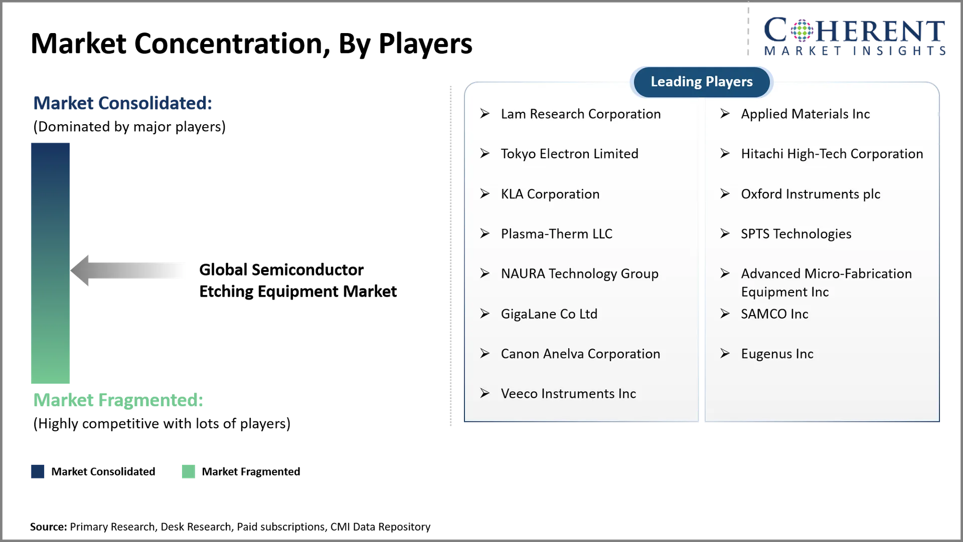
Companies covered: | Lam Research Corporation, Applied Materials Inc, Tokyo Electron Limited, Hitachi High-Tech Corporation, KLA Corporation, Oxford Instruments plc, Plasma-Therm LLC, SPTS Technologies, NAURA Technology Group, Advanced Micro-Fabrication Equipment Inc, GigaLane Co Ltd, SAMCO Inc, Canon Anelva Corporation, Eugenus Inc, Veeco Instruments Inc | ||
Growth Drivers: |
| ||
Restraints & Challenges: |
| ||
Analyst Opinion (Expert Opinion)
- The future of semiconductor etching will center on controlled material removal rather than conventional bulk plasma processing. Gate-All-Around, complementary field-effect transistor, and increasingly vertical memory structures will require selective etching at atomic dimensions. Three-dimensional NAND, high-bandwidth memory, and advanced logic should remain particularly important application areas. The industry will increasingly combine etching with deposition, surface treatment, and metrology. Equipment platforms capable of controlling several related process steps should gain stronger customer relevance.
- The largest opportunity should emerge in selective etching for advanced logic and high-aspect-ratio etching for memory. Gate-All-Around manufacturing requires selective removal of silicon-germanium without damaging surrounding silicon structures. Three-dimensional NAND also creates demanding requirements for deep channel formation and word line separation. Taiwan and South Korea should remain critical opportunity centers because their leading manufacturers continue advancing logic and memory technologies. The U.S. should become increasingly important as domestic advanced-node fabrication expands.
- Equipment manufacturers should prioritize chemistry development, real-time process sensing, and chamber-level uniformity. Lam Research demonstrates the importance of combining selective etching with advanced surface treatments and application-specific platforms. Applied Materials demonstrates another strategic route by combining deposition and selective etching for three-dimensional structures. Suppliers seeking an edge should develop tightly integrated process solutions with semiconductor manufacturers. They should also optimize equipment for new materials, extreme aspect ratios, and lower process damage.
Speak to the analyst
Want personalized insights?
Take the findings above to one of our principal consultants, or have the report rebuilt around the segments, geographies and competitors you actually track.
Market Segmentation
- Etch Type Insights (Revenue, USD Billion, 2021 - 2033)
- Dry Etching
- Wet Etching
- Dimension Insights (Revenue, USD Billion, 2021 - 2033)
- 3D
- 2.5D
- 2D
- Application Insights (Revenue, USD Billion, 2021 - 2033)
- Logic and Memory
- MEMS
- Power Devices
- Others
- Regional Insights (Revenue, USD Billion, 2021 - 2033)
- North America
- U.S.
- Canada
- Latin America
- Brazil
- Argentina
- Mexico
- Rest of Latin America
- Europe
- Germany
- U.K.
- Spain
- France
- Italy
- Russia
- Rest of Europe
- Asia Pacific
- China
- India
- Japan
- Australia
- South Korea
- ASEAN
- Rest of Asia Pacific
- Middle East
- GCC Countries
- Israel
- Rest of Middle East
- Africa
- South Africa
- North Africa
- Central Africa
- North America
- Key Players Insights
- Lam Research Corporation
- Applied Materials Inc
- Tokyo Electron Limited
- Hitachi High-Tech Corporation
- KLA Corporation
- Oxford Instruments plc
- Plasma-Therm LLC
- SPTS Technologies
- NAURA Technology Group
- Advanced Micro-Fabrication Equipment Inc
- GigaLane Co Ltd
- SAMCO Inc
- Canon Anelva Corporation
- Eugenus Inc
- Veeco Instruments Inc
Sources
Primary Research Interviews
- Semiconductor Equipment Manufacturers
- Integrated Device Manufacturers (IDMs)
- Foundry & Fab Operators
- Raw Material & Component Suppliers
Magazines
- Semiconductor Digest
- Solid State Technology
- IEEE Spectrum
- Chip Scale Review
Journals
- Journal of Vacuum Science & Technology
- Journal of The Electrochemical Society
- Microelectronic Engineering (Elsevier)
Associations
- SEMI (Semiconductor Equipment and Materials International)
- Semiconductor Industry Association (SIA)
- JEITA (Japan Electronics and Information Technology Industries Association)
- ESIA (European Semiconductor Industry Association)
Public Domain Sources
- U.S. International Trade Administration (ITA) – Semiconductor Reports
- World Semiconductor Trade Statistics (WSTS)
- U.S. Securities and Exchange Commission (SEC) – Company Filings
- European Commission – Digital Industry Reports
Proprietary Elements
- CMI Data Analytics Tool
- Proprietary CMI Existing Repository of Information for Last 10 Years
Get access to 250+ pages report
Every segment, forecast, competitor profile and data table behind the analysis above — available for instant download.
- ESOMAR Member
- ISO 9001:2015 Certified
- D-U-N-S Registered
- GDPR & CCPA Compliant
Frequently Asked Questions
The global semiconductor etching equipment market is expected to stand at USD 18.00 Bn in 2026 and is expected to reach USD 32.00 Bn by 2033.
The CAGR of the global semiconductor etching equipment market is projected to be 9% from 2026 to 2033.
Expansion of advanced semiconductor fabrication plants and Increasing adoption of three-dimensional semiconductor architectures are the major factors driving the growth of the global semiconductor etching equipment market.
High equipment acquisition costs and Complex equipment maintenance requirements are the major factors hampering the growth of the global semiconductor etching equipment market.
In terms of etch type, dry etching segment is estimated to dominate the market revenue share in 2026.
Semiconductor etching equipment removes selected materials from wafers during semiconductor device fabrication.
Gate-All-Around structures require highly selective etching around vertically arranged semiconductor channels.