

Global Semiconductor Materials Market Size and Forecast – 2026 To 2033
The global semiconductor materials market is expected to grow from USD 90.00 Bn in 2026 to USD 275.50 Bn by 2033, registering a compound annual growth rate (CAGR) of 13.8% from 2026 to 2033. The global semiconductor materials market is driven by expansion of high-bandwidth memory production. On September 12, 2025, SK hynix Inc. announced that it has completed development and finished preparation of HBM4, a next generation memory product for ultra-high-performance AI, mass production for the world’s first time.
Key Takeaways of the Global Semiconductor Materials Market
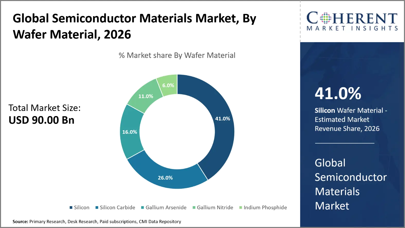
- The Silicon segment is expected to account for 41.0% of the global semiconductor materials market share in 2026. Growing adoption of advanced semiconductor packaging is driving the growth of the segment. On June 25, 2026, Applied Materials introduced new systems for dynamic random-access memory and advanced semiconductor packaging.
- The Wafer Fabrication segment is estimated to capture 37.0% of the market share in 2026. Increasing demand for high-purity silicon wafers is majorly driving the growth of the segment. On June 30, 2025, Okmetic produced its first silicon wafers at its expanded Vantaa facility in Finland. It increases capacity for 200-millimetre polished silicon wafers and supports silicon-on-insulator products.
- The Logic and Microprocessors segment is estimated to capture 33.0% of the market share in 2026. Expansion of electric vehicle semiconductor applications is majorly driving the growth of the segment. On September 4, 2025, ROHM and Schaeffler began mass production of an inverter brick incorporating ROHM's silicon carbide metal-oxide-semiconductor field-effect transistor bare chips.
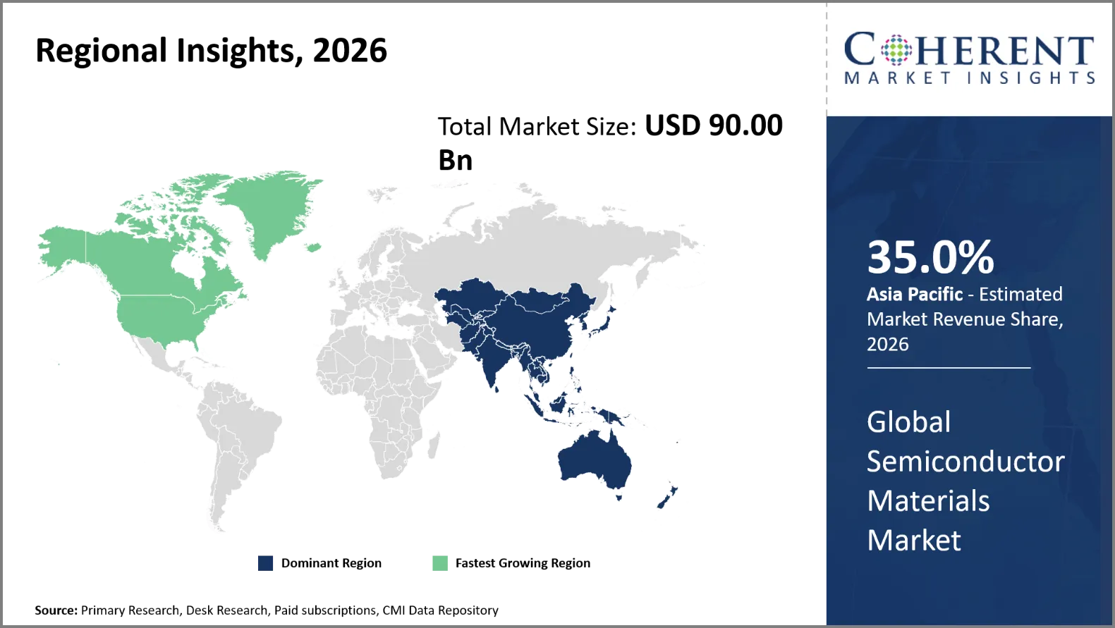
- Asia Pacific is expected to dominate the semiconductor materials market in 2026 with a market share of 35.0%. Adoption of smart monitoring and predictive maintenance technologies in Asia Pacific is driving the growth of the regional market. On October 6, 2025, Schaeffler launched its Asia Pacific Remote Monitoring Center in Singapore to help industrial customers improve equipment reliability.
- North America is expected to account for 26.0% share in 2026 and is projected to record the fastest growth over the forecast period. Expansion of waste incineration and biomass power projects in North America is driving the growth of the regional market. On January 14, 2026, NewYork GreenCloud announced its acquisition of the Buena Vista Biomass Power facility in Ione, California. The company plans to expand the existing 18-megawatt plant into a 41-megawatt power facility.
Segmental Insights
Why Does Silicon Dominate the Global Semiconductor Materials Market?
The silicon segment is expected to account for 41.0% of the global semiconductor materials market share in 2026. Silicon is dominant owing to its good electrical qualities, its abundance in nature, and its developed manufacturing processes. It can be doped to act as a semiconductor and engineered into transistors to precisely control electrical conductivity. Silicon also forms a stable layer of silicon dioxide that allows effective insulating and gate designs in integrated circuits. Industrial significance is reinforced by established wafer production techniques, broad supplier networks, and interoperability with complementary metal-oxide-semiconductor technologies. Manufacturers widely employ silicon wafers in processors, memory chips, power management integrated circuits and automotive electronics.
On May 16, 2025, GlobalWafers built a new silicon wafer manufacturing plant in Sherman Texas, U.S. The company invested almost USD 3.5 billion in the facility that makes sophisticated 300mm silicon wafers. It also announced plans for an additional USD 4 billion investment in the U.S. semiconductor industry.
- Current Industry Events of 2026
- Market Size Estimation
- Regional Breakdown
- Competitive Landscape
- Customer Intelligence
- Segmental Analysis
- Pricing Analysis
- Key Market Drivers, Challenges & Future Trends
- Customized Insights Section
Why is Wafer Fabrication the Most Crucial Manufacturing Process?
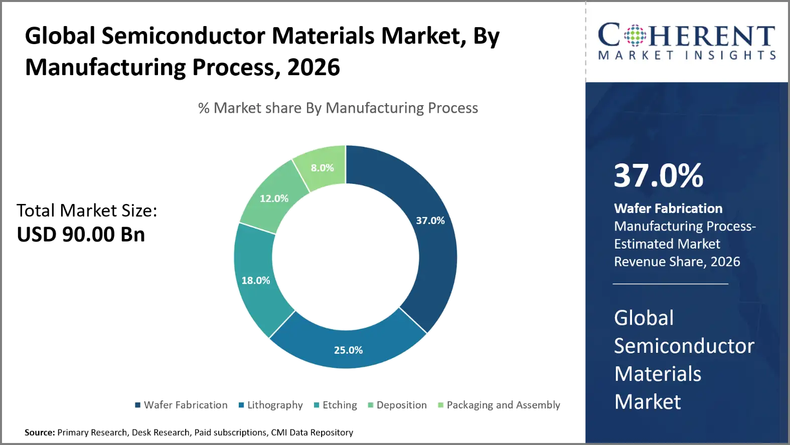
The wafer fabrication segment is expected to account for 37.0% of the global semiconductor materials market share in 2026. Wafer fabrication is the most crucial semiconductor manufacturing process because it creates the functional electronic structures within integrated circuits. The process consists of repeated phases of deposition, photolithography, etching, doping and cleaning on semiconductor wafers. These activities define the transistor architecture and electrical connections that determine chip performance, power consumption and reliability. Defects at the microscopic level diminish the manufacturing yield and raise the production cost. Thus, accurate process control is required for advanced fabrication. The demand for artificial intelligence accelerators, high-performance computing processors and enhanced memory drives the need for sophisticated wafer production.
On January 27, 2026, Micron Technology, Inc. began construction on an upgraded wafer fabrication facility at the company’s current NAND manufacturing complex in Singapore. This new facility represents a planned investment of approximately USD 24 billion over 10 years and is designed to ultimately provide 700,000 square feet of cleanroom space.
Logic and Microprocessors Dominates the Global Semiconductor Materials Market
The logic and microprocessors segment is expected to account for 33.0% of the global semiconductor materials market share in 2026. Logic and microprocessors represent a major application segment of the global semiconductor materials market because they power computing, communication, and intelligent electronic systems. These devices require silicon wafers, photoresists, specialty gasses, deposition precursors, etchants and high-purity process chemicals. Advanced processors with complex transistor architectures are in demand driven by cloud computing and artificial intelligence infrastructure. More sophisticated logic chips are also required in automotive electronics, smartphones, industrial automation and networking equipment. The shrinking of the transistor sizes and the sophisticated packaging technologies impose new demands for the precision of the material design and contaminant control.
On October 9, 2025, Intel announced that its Panther Lake processors are in production using its Intel 18A process. The company identified Fab 52 in Chandler, Arizona, U.S., as the facility supporting high-volume production. Intel 18A combines RibbonFET gate-all-around transistors with PowerVia backside power delivery.
Current Events and their Impact
Current Events | Description and its Impact |
U.S. CHIPS and Science Act, Public Law 117-167 |
|
U.S. Semiconductor Export Controls, Federal Register citation 89 FR 96790 |
|
Semiconductor Materials Market Dynamics
Market Drivers
Increasing semiconductor fabrication capacity
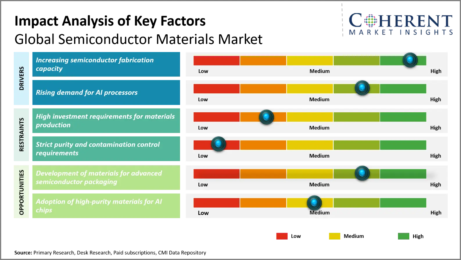
The growth of semiconductor fabrication capacity is creating demand for silicon wafers, photoresists, specialized gasses, deposition chemicals and high-purity wet processing materials. Semiconductor companies are building new fabs and extending existing lines of production to shore up supply-chain resiliency. Such facilities require large quantities of carefully designed materials for wafer preparation, transistor generation, cleaning, and connection production. Advanced process nodes also require better contamination control and more sophisticated chemical formulations. Several countries are promoting capacity building through government incentives and regional manufacturing initiatives. Thus, the increase in fabrication generates more opportunity for semiconductor material manufacturers.
On March 4, 2025, TSMC announced its intention to expand its investment in advanced semiconductor manufacturing in the U.S. by an additional USD 100 billion. Building on the company’s ongoing USD 65 billion investment in its advanced semiconductor manufacturing operations in Phoenix, Arizona, TSMC’s total investment in the U.S. is expected to reach USD 165 billion.
Rising demand for AI processors
Increasing demand for artificial intelligence processors is driving the usage of advanced semiconductor materials used in high-performance computing chips and accelerator devices. AI workloads demand powerful processors with complicated transistor topologies, dense interconnects, and innovative packaging architectures. These technologies rely on high-quality silicon wafers, sophisticated photoresists, deposition precursors, etchants and specialized cleaning solvents. The increasing demand for high bandwidth memory and chiplet-based architectures further drives the demand for innovative packaging materials and high-density substrates. Cloud service providers and semiconductor manufacturers are building up AI infrastructure to support model training and inference.
On March 11, 2026, Meta announced plans to develop and roll out four new versions of its Meta Training and Inference Accelerator chips over the next two years. The roadmap includes MTIA 300, MTIA 400, MTIA 450 and MTIA 500. MTIA 300 is in production for ranking and recommendation training.
Emerging Trends
- Advanced Packaging Materials: The demand for advanced packaging technologies like chiplets and 3D integration is driving the need for high-performance substrates, dielectric materials, bonding materials, and specialty encapsulants throughout semiconductor manufacturing.
- Impact: These technologies increase material complexity and purity requirements, and drive providers to produce solutions that support heat management, electrical connectivity, and reliable integration of multiple semiconductor die.
- Relevance to the market: Advanced packaging creates new opportunities for materials suppliers that can provide high density substrates, underfill materials, bonding compounds and dielectric films for artificial intelligence processors and high-performance computer applications.
- High-Purity Semiconductor Materials: As transistor sizes decrease, semiconductor manufacturers are seeking ultra-high-purity chemicals, specialty gasses and sophisticated photoresists to meet tighter requirements for contamination control and process precision.
- Impact: Increased quality-control expenses, specialized purification technologies, and supplier certification requirements across wafer fabrication and advanced semiconductor manufacturing processes due to higher purity requirements.
- Relevance to the market: Ultra-high purity materials are required from specialized vendors for advanced fabrication nodes, higher manufacturing yields and strict performance requirements throughout future generation semiconductor devices.
Regional Insights
Why is Asia Pacific a Strong Market for Semiconductor Materials?
Asia Pacific is expected to account for a market share of 35.0% in 2026. Semiconductor fabrication, sophisticated packaging and memory manufacturing in the Asia Pacific region are concentrated in a number of economies. Taiwan's foundries make advanced logic using specialized photoresists, silicon wafers and deposition chemicals. South Korea’s memory makers require high-purity materials for dynamic random-access memory and high-bandwidth memory. Japan Increases Supply of Silicon Wafers, Photoresists, Semiconductor Grade Chemicals in Region. Demand for locally manufactured materials is underpinned by investments in domestic production in China. India's semiconductor push is opening prospects for electronic gasses, wafer processing chemicals and packaging supplies. Regional demand increasingly reflects advanced packaging, memory expansion, and domestic semiconductor supply-chain development.
Why Does North America Semiconductor Materials Market Exhibit High Growth?
North America, registering the fastest growth with a CAGR of 14.1% over the forecast period, is projected to account for 26.0% of the global semiconductor materials market in 2026. North America benefits from semiconductor supply-chain localization, particularly through investments in domestic fabrication and advanced packaging infrastructure. Taiwan Semiconductor Manufacturing Company proposes more Arizona fabs, advanced packaging units and research infrastructure. GlobalFoundries has said it will invest in New York and Vermont to build semiconductor production and advanced packaging capabilities. Micron Technology is growing its memory production and research operations in Idaho, New York and Virginia. These projects create a demand for domestic silicon wafers, photoresists, specialty gasses, polishing slurries and high-purity chemicals. New fabrication facilities increasingly benefit from certification requirements and lower delivery distances for regional suppliers.
Global Semiconductor Materials Market Outlook for Key Countries
Why is China Emerging as a Major Hub in the Semiconductor Materials Market?
Both domestic sourcing strategies and efforts to build up indigenous semiconductor manufacturing skills are factors in China’s semiconductor materials market. Semiconductor producers need local availability of silicon wafers, electronic chemicals, specialty gasses, photoresists and deposition materials. Domestic producers are working on materials that support fabrication processes and lessen reliance on international procurement. Established firms also need chemical mechanical planarization slurries and innovative packaging materials for ever more complex electronics. Restrictions on access to some foreign technologies result in the further development and certification of indigenous suppliers. Demand from cellphones, telecommunications equipment, automotive electronics and computing applications are supported by China’s massive electronics manufacturing base.
Is U.S. the Next Growth Engine for the Semiconductor Materials Market?
Advanced artificial intelligence infrastructure and investment in domestic memory fabrication support the U.S. market for semiconductor materials. In June 2025, Micron Technology announced plans for a major manufacturing and research expansion in New York, Virginia and Idaho. The program comprises more fabrication facilities and enhanced high-bandwidth memory packing. Taiwan Semiconductor Manufacturing Company also increased its planned investment in Arizona, including more fabrication factories and packaging facilities. These projects require qualified suppliers of silicon wafers, deposition precursors, photoresists, specialty gasses and advanced packaging materials. The rise of domestic manufacturing also causes materials businesses to build technical assistance and supply operations close to fabrication locations.
Taiwan Semiconductor Materials Market Analysis and Trends
The continuous development of improved chip fabrication technologies and advanced foundry manufacturing is good for Taiwan’s semiconductor materials business. Taiwan Semiconductor Manufacturing Company makes chips for customers designing artificial intelligence processors, graphics processing units and high-performance computing devices. These applications demand high precision lithography materials, chemical mechanical planarization slurries, high purity cleaning chemicals and advanced packaging substrates. Fujifilm said it plans to invest about 15 billion yen in semiconductor materials facilities in Taiwan. Its projects include chemical mechanical planarization slurries and materials related to photolithography and will build new production bases in Hsinchu and Tainan. Local production of materials encourages closer technical collaboration, faster certification, and stable supply for advanced semiconductor fabrication.
Japan Semiconductor Materials Market Analysis and Trends
Japan’s semiconductor materials business is underpinned by specialist materials engineering, proven chemical production expertise and research alliances driving next-generation fabrication. Key suppliers of wafer and process materials include Shin-Etsu Chemical, SUMCO, Tokyo Ohka Kogyo and Fujifilm. Fujifilm’s investment in Rapidus, finalized in February 2026, was part of Japan’s efforts to build its capacity in advanced logic production. The company also said it wants to further invest in semiconductor material development and manufacturing capabilities. Japanese vendors are particularly pertinent to high-purity silicon wafers, sophisticated photoresists, polishing slurries, post-polishing cleansers and polyimides. Their customized formulations facilitate high resolution lithography, defect reduction and reliable processing for modern semiconductor devices.
South Korea Semiconductor Materials Market Analysis and Trends
South Korea’s semiconductor materials market is driven by the advanced memory manufacturing industry, especially the creation of high bandwidth memory and 3D NAND flash. Complex memory structures need unique deposition precursors, etchants, cleaning chemicals and sputtering targets from Samsung Electronics and SK hynix. SK hynix announced a major Yongin semiconductor cluster investment in February 2026, including additional cleanroom development. JX Advanced Metals also announced an investment in South Korean sputtering-target processing capacity in July 2026. These targets support advanced logic and memory manufacturing. Such developments strengthen demand for materials that improve thin-film uniformity, interconnect performance, and manufacturing consistency across increasingly complex memory devices.
Global Semiconductor Materials Market - High-Bandwidth Memory Packaging Materials
Material | Key Function | Data Point | Application in HBM Packaging |
High-thermal-conductivity epoxy molding compound | Protects memory dies and improves heat transfer | 3.5 times higher thermal conductivity and 47% lower vertical thermal resistance reported by SK hynix | Mobile stacked memory and heat-sensitive semiconductor packages |
Integrated cooling elements | Adds a thermal pathway inside the memory package | 30% reduction in thermal resistance reported by SK hynix | Next-generation high-bandwidth memory and high-performance computing |
Through-silicon via dielectric liners | Electrically insulates vertical connections through silicon dies | Uniform low-temperature dielectric deposition along high-aspect-ratio via sidewalls | Vertical electrical connections in stacked DRAM dies |
Barrier and seed layers | Enables reliable copper deposition inside vertical vias | Barrier and seed layer coverage and continuity are critical for electrical performance and reliability | Through-silicon vias and stacked-memory interconnects |
Under-bump metallization | Supports electrical connection between stacked dies | Contact resistance and bump reliability become more challenging as bump dimensions shrink | Micro-bump interconnections in high-bandwidth memory stacks |
How is Development of Materials for Advanced Semiconductor Packaging Creating New Growth Opportunities in the Semiconductor Materials Market?
Development of materials for advanced semiconductor packaging is creating growth opportunities by addressing the thermal, electrical, and integration challenges of artificial intelligence processors and high-bandwidth memory. Hybrid bonding requires exceptionally clean copper surfaces and precise dielectric interfaces to enable finer interconnects between stacked semiconductor dies. Increasing demand for photosensitive dielectrics, plating chemicals and fine-line patterning materials is being driven by advanced redistribution layers. Silicon interposers and glass substrates also provide new prospects for metallization chemicals, adhesion boosters and low loss dielectric materials. Underfill compounds and molding materials also need to survive thermal cycling without impacting package dependability. Suppliers creating low-warpage substrates, thermally conductive encapsulants and bonding materials can satisfy chiplet integration and 3D packaging requirements.
On September 29, 2025, FUJIFILM Corporation announced the launch of CMP slurry for advanced packaging, enabling the integration of multiple semiconductor chips into a single package. This product has been adopted by a major semiconductor device manufacturer as an essential abrasive for planarizing bonding surfaces in hybrid bonding, one of the advanced packaging technologies for enhancing AI semiconductor performance.
Market Players, Key Development, and Competitive Landscape
Key Developments
- On June 19, 2026, Tokuyama Corporation announced that Hantok Chemicals Co., Ltd., an equity-method affiliate of Tokuyama, held a groundbreaking ceremony in South Korea, for its new Pyeongtaek Plant, which will be a new production facility for tetramethylammonium hydroxide (TMAH), a photoresist developer.
- On April 9, 2026, Sumitomo Chemical announced plans to construct a new facility that integrates photoresist manufacturing process technology management, quality evaluation, and analytical functions at its Osaka Works, located in Osaka, Japan. The facility is planned to further strengthen Sumitomo Chemical’s supply system for photoresists for advanced semiconductors, including extreme ultraviolet and argon fluoride photoresists.
- On March 5, 2026, Air Liquide unveiled the successful construction of its new Advanced Materials manufacturing plant in Taichung City, Taiwan. Already present in this key innovative market with 54 facilities dedicated to the semiconductor industry in Taiwan, this is the first large-scale Air Liquide production site of advanced deposition and etching materials in Taiwan.
Competitive Landscape
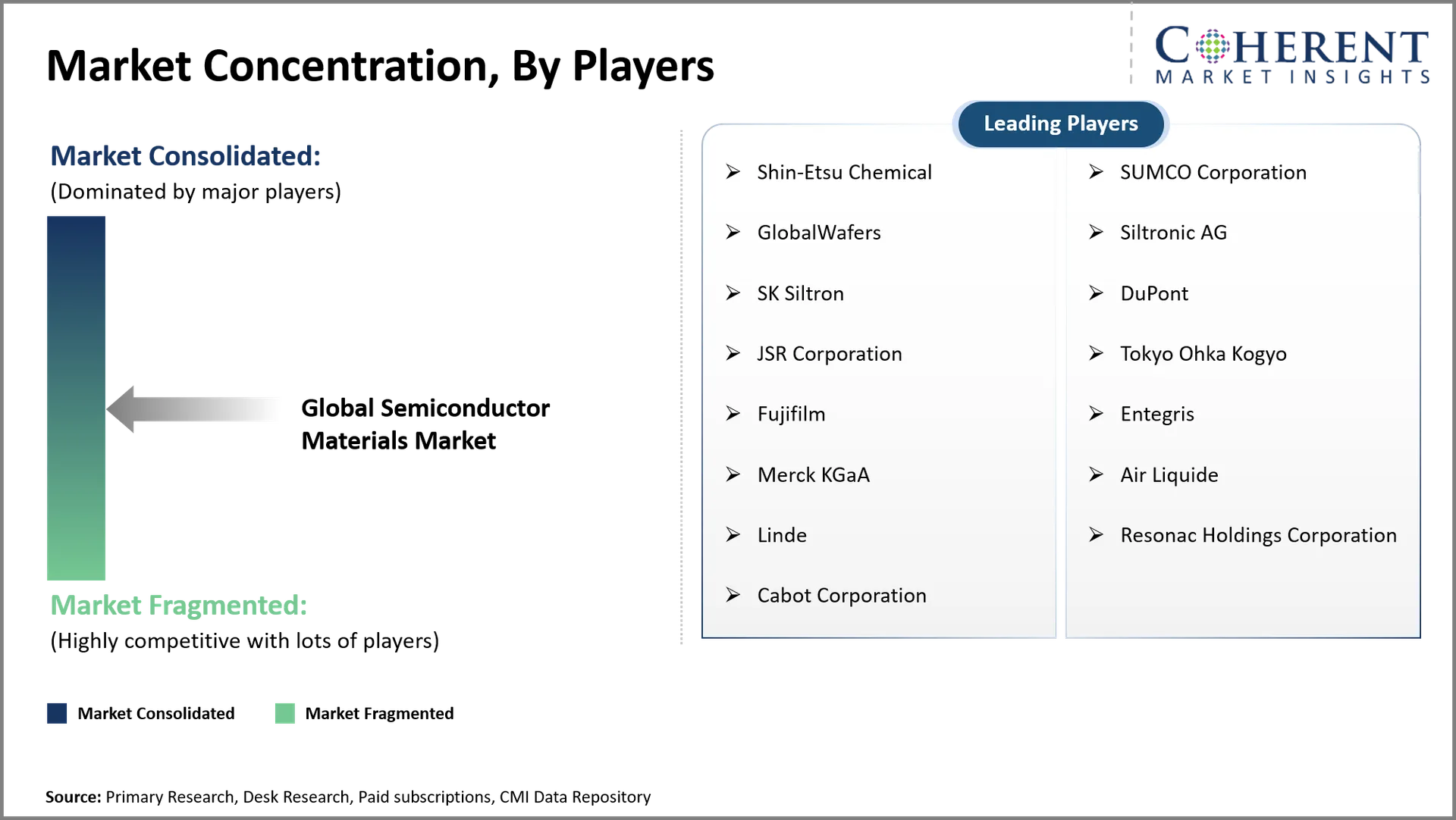
The global semiconductor materials market is shaped by suppliers competing through material purity, process compatibility, research partnerships, and regional manufacturing expansion. Fujifilm is expanding its Mesa, Arizona, facility with an USD 18 million investment for copper interconnect polishing slurries and advanced packaging materials. Entegris announced a USD 700 million investment in U.S. research and development, including a technology center in Illinois that will work on deposition materials, polishing slurries, cleaning solutions and polishing pads. JSR Corporation and Entegris additionally entered into a cross-licensing arrangement for metal oxide photoresists used in severe UV lithography. Meanwhile, Shin-Etsu Chemical and SUMCO are strategically placed in silicon wafers, while Tokyo Ohka Kogyo is a specialist in photoresists. The enterprises focus on sophisticated fabrication needs, client validation and reliable supply.
Top Manufacturers and Notable Products in the Semiconductor Materials Market
Manufacturer | Notable Product | Key features |
Ajinomoto Fine-Techno Co., Inc. | Ajinomoto Build-up Film (ABF) | Insulating build-up film for high-density package substrates, supports fine wiring and multilayer interconnections in advanced processors |
Resonac Holdings Corporation | Semiconductor Packaging Materials Portfolio | Provides encapsulation materials, copper-clad laminates, and interposer-related materials for advanced multi-chip packaging |
Henkel AG & Co. KGaA | LOCTITE Semiconductor Packaging Materials | Includes underfills, die-attach materials, encapsulants, and adhesives designed for package protection and mechanical reliability |
NAMICS Corporation | Liquid Compression Molded Underfill (LCMUF) | Supports wafer-level and panel-level packaging, fast curing, and reduced warpage after molding |
Sumitomo Bakelite Co., Ltd. | Epoxy Molding Compounds | Provides encapsulation and protection for semiconductor packages, supporting reliability and resistance to environmental stress |
Semiconductor Materials Market Report Coverage | |||
Report Coverage | Details | ||
Base Year | 2025 | Market Size in 2026: | USD 90.00 Bn |
Historical Data For: | 2020 To 2024 | Forecast Period: | 2026 To 2033 |
Forecast Period 2026 To 2033 CAGR: | 13.8% | 2033 Value Projection: | USD 275.50 Bn |
Geographies covered: |
| ||
Segments covered: |
| ||
Companies covered: | Shin-Etsu Chemical, SUMCO Corporation, GlobalWafers, Siltronic AG, SK Siltron, DuPont, JSR Corporation, Tokyo Ohka Kogyo, Fujifilm, Entegris, Merck KGaA, Air Liquide, Linde, Resonac Holdings Corporation, Cabot Corporation | ||
Growth Drivers: |
| ||
Restraints & Challenges: |
| ||
Analyst Opinion (Expert Opinion)
- The future of the semiconductor materials industry will depend increasingly on advanced packaging, high-bandwidth memory, and increasingly complex artificial intelligence processors. Hybrid bonding, three-dimensional integration, and chiplet architectures will require specialized polishing slurries, dielectric materials, bonding films, and high-purity process chemicals. Fujifilm's planned expansion of hybrid-bonding-related polishing capabilities illustrates how suppliers are adapting their portfolios to these manufacturing requirements.
- The strongest opportunities will emerge in advanced packaging materials, extreme ultraviolet lithography materials, and high-purity chemicals for leading-edge fabrication. Taiwan and South Korea offer opportunities around advanced foundries and memory production, while the U.S. presents opportunities through domestic fabrication and packaging expansion. Japan remains strategically important for silicon wafers, photoresists, and specialized chemical formulations. Suppliers should prioritize materials that improve bonding precision, reduce contamination, and maintain performance under demanding thermal conditions.
- Market participants should develop application-specific formulations alongside semiconductor manufacturers and packaging specialists. Early qualification with fabrication facilities can improve adoption prospects and reduce the risk of delayed production integration. Companies also need to develop regional technical support and production capacity around large semiconductor clusters. Investment should be concentrated on hybrid bonding, low-loss dielectric materials, improved photoresists, and sustainable chemical purification. Suppliers that can supply consistent quality, reliable delivery and fast joint development can build better client connections and differentiate their portfolios.
Speak to the analyst
Want personalized insights?
Take the findings above to one of our principal consultants, or have the report rebuilt around the segments, geographies and competitors you actually track.
Market Segmentation
- Wafer Material Insights (Revenue, USD Billion, 2021 - 2033)
- Silicon
- Silicon Carbide
- Gallium Arsenide
- Gallium Nitride
- Indium Phosphide
- Manufacturing Process Insights (Revenue, USD Billion, 2021 - 2033)
- Wafer Fabrication
- Lithography
- Etching
- Deposition
- Packaging and Assembly
- Application Insights (Revenue, USD Billion, 2021 - 2033)
- Logic and Microprocessors
- Memory Devices
- Analog Integrated Circuits
- Discrete Devices
- Power Semiconductors
- Others
- End User Insights (Revenue, USD Billion, 2021 - 2033)
- Consumer Electronics
- Automotive
- Telecommunications
- Data Centers
- Industrial Electronics
- Others
- Regional Insights (Revenue, USD Billion, 2021 - 2033)
- North America
- U.S.
- Canada
- Latin America
- Brazil
- Argentina
- Mexico
- Rest of Latin America
- Europe
- Germany
- U.K.
- Spain
- France
- Italy
- Russia
- Rest of Europe
- Asia Pacific
- China
- India
- Japan
- Australia
- South Korea
- ASEAN
- Rest of Asia Pacific
- Middle East
- GCC Countries
- Israel
- Rest of Middle East
- Africa
- South Africa
- North Africa
- Central Africa
- North America
- Key Players Insights
- Shin-Etsu Chemical
- SUMCO Corporation
- GlobalWafers
- Siltronic AG
- SK Siltron
- DuPont
- JSR Corporation
- Tokyo Ohka Kogyo
- Fujifilm
- Entegris
- Merck KGaA
- Air Liquide
- Linde
- Resonac Holdings Corporation
- Cabot Corporation
Sources
Primary Research Interviews
- Semiconductor Material Manufacturers & Suppliers
- Wafer Fabrication Specialists
- Semiconductor Equipment Providers
- Electronic Component Distributors & OEMs
Magazines
- Semiconductor Digest
- Electronic Design Magazine
- Solid State Technology
- IEEE Spectrum
Journals
- Journal of Electronic Materials (Springer)
- Journal of the Electrochemical Society
- Microelectronic Engineering (Elsevier)
Associations
- SEMI (Semiconductor Equipment and Materials International)
- Semiconductor Industry Association (SIA)
- JEDEC Solid State Technology Association
- Global Semiconductor Alliance (GSA)
Public Domain Sources
- U.S. Geological Survey (USGS) - Critical Minerals & Materials Data
- World Semiconductor Trade Statistics (WSTS)
- U.S. International Trade Commission (USITC) Reports
- European Commission - Digital Economy & Society Reports
Proprietary Elements
- CMI Data Analytics Tool
- Proprietary CMI Existing Repository of information for last 10 years
Get access to 250+ pages report
Every segment, forecast, competitor profile and data table behind the analysis above — available for instant download.
- ESOMAR Member
- ISO 9001:2015 Certified
- D-U-N-S Registered
- GDPR & CCPA Compliant
Frequently Asked Questions
The global semiconductor materials market is expected to stand at USD 90.00 Bn in 2026 and is expected to reach USD 275.50 Bn by 2033.
The CAGR of the global semiconductor materials market is projected to be 13.8% from 2026 to 2033.
Increasing semiconductor fabrication capacity and Rising demand for AI processors are the major factors driving the growth of the global semiconductor materials market.
High investment requirements for materials production and Strict purity and contamination control requirements are the major factors hampering the growth of the global semiconductor materials market.
In terms of wafer material, silicon segment is estimated to dominate the market revenue share in 2026.
Semiconductor materials are specialized substances used to manufacture wafers, transistors, integrated circuits, and advanced electronic components.
Specialty gases support deposition, etching, chamber cleaning, and doping processes that establish precise semiconductor device structures.