

Global Hybrid Bonding Market Size and Forecast – 2026 To 2033
The global hybrid bonding market is expected to grow from USD 200.0 Mn in 2026 to USD 931.0 Mn by 2033, registering a compound annual growth rate (CAGR) of 18.0% from 2026 to 2033. The market for hybrid bonding is driven by increasing chiplet integration in artificial intelligence processors. On May 29, 2026, CoAsia unveiled the latest roadmap for its next-generation chiplet packaging platform, CoCs (CoAsia Chiplet Solution), at Samsung Foundry’s SAFE Forum 2026 held in Silicon Valley. CoAsia Semi’s CoCs is a platform that partitions a single chip into functional dies and applies optimized process technologies and packaging architectures to each die.
Key Takeaways of the Global Hybrid Bonding Market
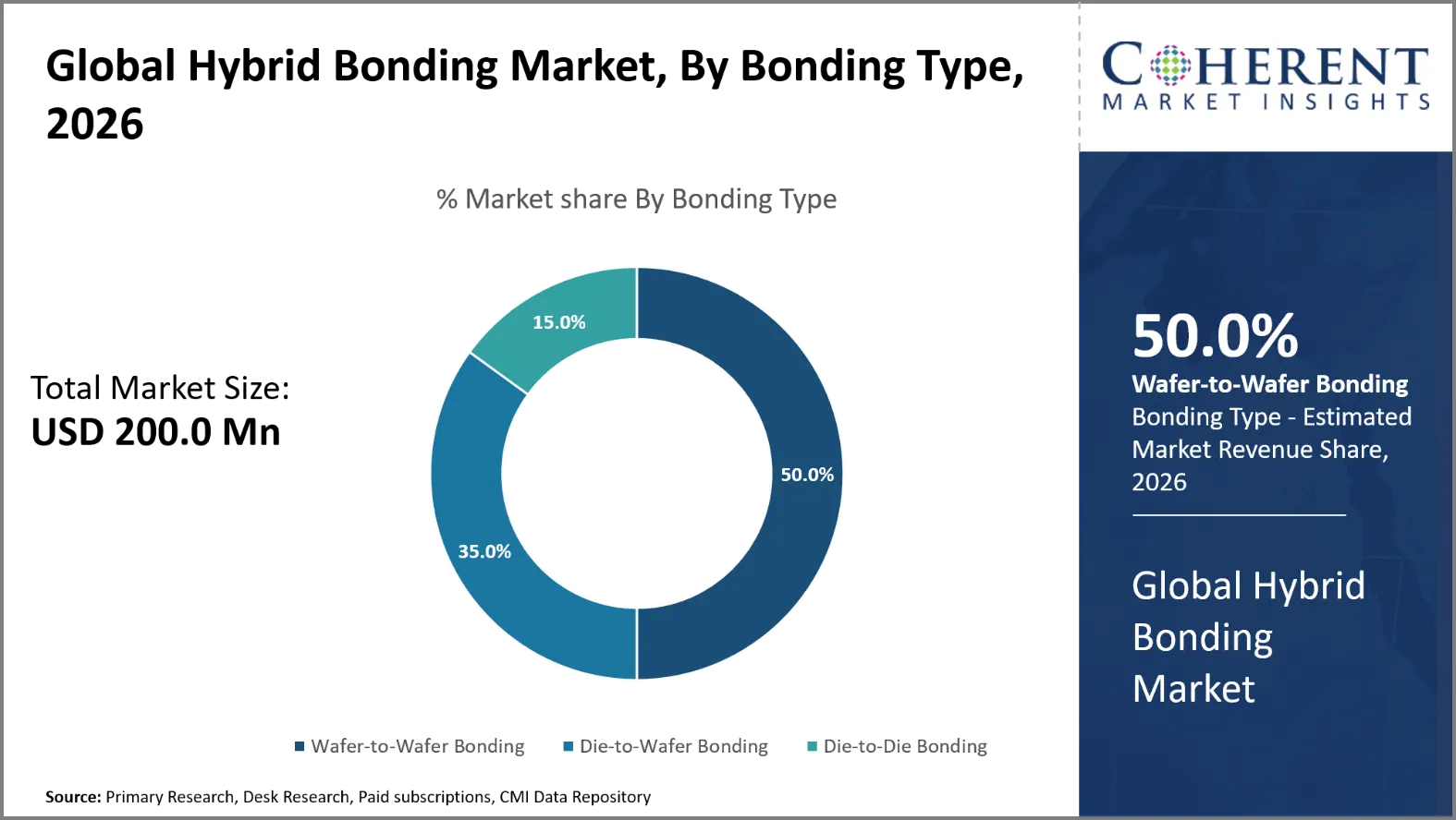
- The Wafer-to-Wafer Bonding segment is expected to account for 50.0% of the global hybrid bonding market share in 2026. Higher interconnect density requirements in advanced semiconductor devices is driving the growth of the segment. On May 28, 2026, imec and EV Group demonstrated wafer-to-wafer hybrid bonding at a 200-nanometer copper interconnect pitch. EV Group's innovative wafer bonding technology delivered record copper-pad alignment precision during the demonstration.
- The Wafer Bonders segment is estimated to capture 42.0% of the market share in 2026. Growing demand for lower power consumption and shorter interconnect lengths is majorly driving the growth of the segment. On June 11, 2025, Marvell Technology launched its custom UALink scale-up solution for AI infrastructure. The solution focuses on low-latency, high-compute-utilization communication between AI accelerators and switches.
- The 3D Integrated Circuits segment is estimated to capture 29.0% of the market share in 2026. Growing investment in advanced packaging manufacturing capacity is majorly driving the growth of the segment. On October 6, 2025, Amkor Technology broke ground on its advanced packaging and test campus in Arizona, U.S. The company expanded the planned investment to USD 7 billion across two phases.
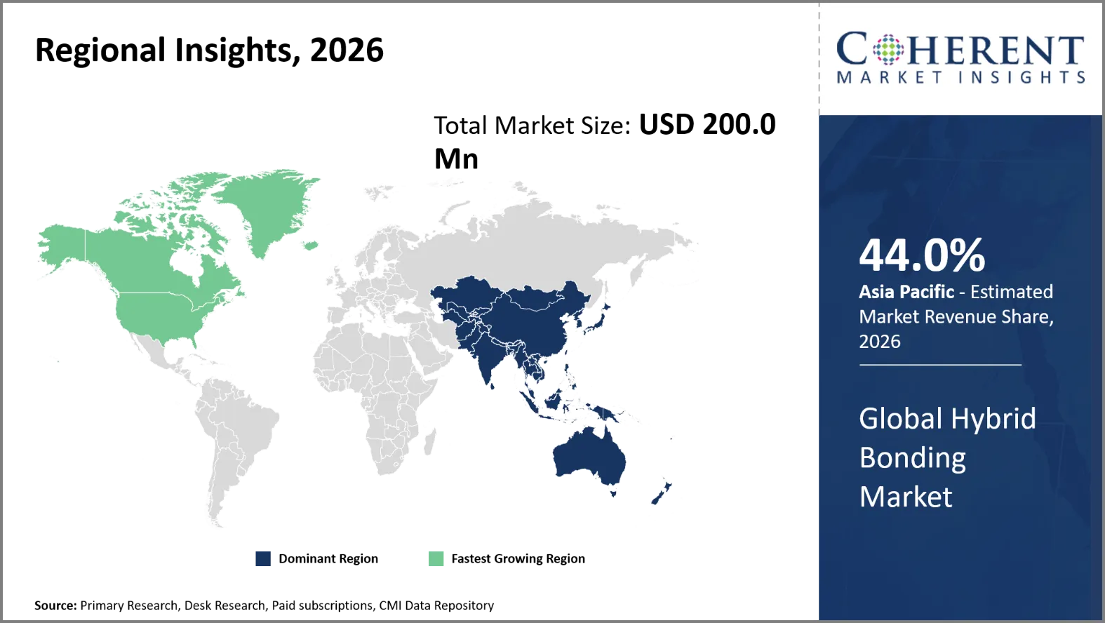
- Asia Pacific is expected to dominate the hybrid bonding market in 2026 with a market share of 44.0%. Increasing demand for 3D integrated circuits in Asia Pacific is driving the growth of the regional market. On August 4, 2026, Samsung Electronics introduced a new 3D memory architecture through its zHBM concept. The architecture vertically positions HBM directly above artificial intelligence accelerators rather than placing memory beside the processor.
- North America is expected to account for 29.0% share in 2026 and is projected to record the fastest growth over the forecast period. Greater use in artificial intelligence and high-performance computing in North America is driving the growth of the regional market. In April 2025, NVIDIA expanded U.S. AI supercomputer manufacturing. NVIDIA began producing Blackwell chips at TSMC’s Arizona facilities. It also established supercomputer manufacturing plants with Foxconn and Wistron in Texas.
Segmental Insights
Why Does Wafer-to-Wafer Bonding Dominate the Global Hybrid Bonding Market?
The wafer-to-wafer bonding segment is expected to account for 50.0% of the global hybrid bonding market share in 2026. Wafer-to-wafer bonding is a high-volume semiconductor manufacturing technology with the ability to align wafers with great precision. The method enables sophisticated 3D integration and dense connection creation. This enhances the production efficiency of businesses who have to process similar structures over full wafers. Wafer-to-wafer bonding also facilitates handling over individual die processing. The growing demand for sophisticated logic, memory and heterogeneous integration further drives the adoption. Manufacturers are moving to wafer-level bonding for improved packaging and three-dimensional integrated circuits. For example, TSMC began volume manufacturing of 3nm SoIC stacking in 2025. SoIC is used for high-density 3D integration by Taiwan Semiconductor Manufacturing Company Limited. The technology targets high-performance computing products and chiplet architectures. TSMC also plans volume production of its COUPE technology in 2026.
- Current Industry Events of 2026
- Market Size Estimation
- Regional Breakdown
- Competitive Landscape
- Customer Intelligence
- Segmental Analysis
- Pricing Analysis
- Key Market Drivers, Challenges & Future Trends
- Customized Insights Section
Why is Wafer Bonders the Most Crucial Equipment Type?
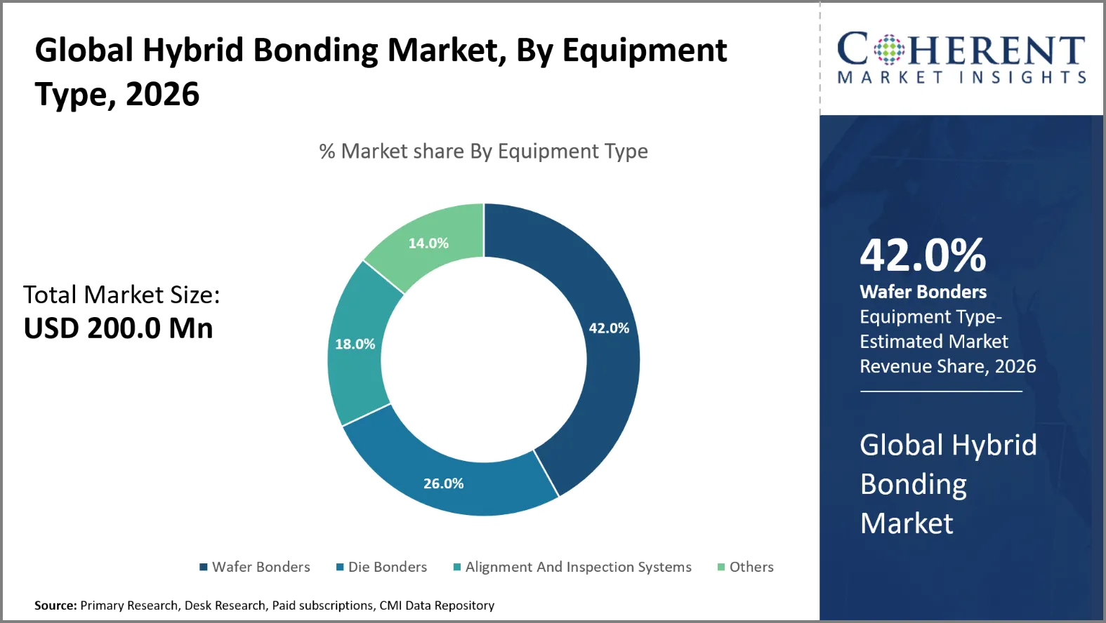
The wafer bonders segment is expected to account for 42.0% of the global hybrid bonding market share in 2026. Wafer bonders are the most important equipment kind, because they manage the alignment, bonding pressure, temperature and surface contact. The accuracy of these directly affects the bond quality, yield and the performance of the semiconductor device. State-of-the-art wafer bonders offer nanoscale scale alignment required for advanced hybrid bonding applications. They provide uniform bonding over broad wafer areas in high volume semiconductor fabrication. Device manufacturers are also expanding their capacities to automate, monitor processes and detect defects. These advances enable semiconductor makers to increase yield and reduce loss in production.
On May 26, 2025, SUSS introduced the XBC300 Gen2 D2W platform, a tailored bonding solution completing the company’s hybrid bonding offering. This new platform further solidifies SUSS’ status as an industry leader in the provision of a fully integrated D2W hybrid bonding solution to meet rigorous manufacturing needs.
3D Integrated Circuits Dominates the Global Hybrid Bonding Market
The 3D integrated circuits segment is expected to account for 29.0% of the global hybrid bonding market share in 2026. 3D integrated circuits dominate as hybrid bonding enables extremely dense vertical interconnections. The technology connects semiconductor layers without conventional solder-based interconnect structures. This allows for shorter electrical lines and enhanced signal performance between the stacked semiconductor layers. Hybrid bonding also enables better connectivity density in ever more compact semiconductor packages. These features are highly beneficial for 3D integrated circuits in advanced computing applications. Artificial intelligence accelerators and high-performance CPUs are progressively demanding higher bandwidth and energy efficiency. Direct copper-to-copper and dielectric bonding are also desirable for memory stacking applications. For example, in 2025, Sony Semiconductor Solutions developed a three-layer 3D heterogeneous structure. Sony presented face-to-back copper-to-copper hybrid bonding using chip-on-wafer integration. The process achieved approximately 99% connection success for 1.4-micrometer pads.
Current Events and their Impact
Current Events | Description and its Impact |
U.S. Advanced Semiconductor Export Controls 15 CFR Part 744 |
|
European Union Chips Act Regulation (EU) 2023/1781 |
|
Hybrid Bonding Market Dynamics
Market Drivers
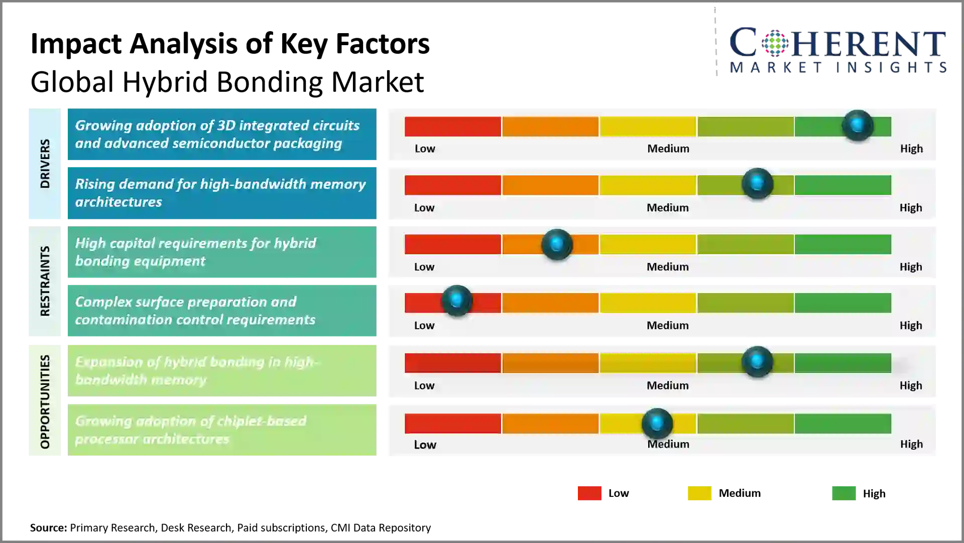
- Growing adoption of 3D integrated circuits and advanced semiconductor packaging: The increasing penetration of three-dimensional integrated circuits is fueling the need for hybrid bonding technologies. Three-dimensional architectures stack numerous layers of semiconductor material into small containers. Hybrid bonding permits direct stacking of dies with ultra-fine connector pitches. This technique enhances bandwidth, decreases interconnect lengths, and enables a higher density of components. Advanced packaging is of growing importance for artificial intelligence processors, high-performance computing and advanced memory devices. Chiplets are the new way for semiconductor makers to combine different functional dies in a single package.
- On May 26, 2026, Advanced Semiconductor Engineering, Inc. announced the launch of the industry’s first automated 310mm x 310mm panel-level packaging production line on May 26, 2026, cementing its position as a leader in next-generation advanced packaging technology. This milestone adds economies of scale by enabling a smooth transition from wafer level packaging to panel level packaging.
- Rising demand for high-bandwidth memory architectures: Growing demand for high-bandwidth memory is leading to the introduction of hybrid bonding for vertically stacked memory designs. The applications of artificial intelligence and high-speed computing demand more memory bandwidth and increased energy efficiency. High bandwidth memory stacks numerous storage dies within small packages to gain increased performance. Hybrid bonding allows for smaller vertical interconnects than standard packaging methods. It can increase the link density and reduce the electrical distances between the stacked memory layers. Memory makers are exploring new stacking techniques to help accommodate the ever-demanding artificial intelligence workloads.
- On May 29, 2026, Samsung Electronics announced that it has begun exporting the world’s first 12-layer HBM4E samples to leading worldwide clients, further solidifying its leadership in the next-generation HBM market.
Emerging Trends
- AI-Driven Advanced Packaging: AI workloads are driving demand for high-density semiconductor packaging. Hybrid bonding allows shorter interconnects, higher bandwidth and better energy efficiency. More semiconductor makers are combining hybrid bonding with three-dimensional structures for improved computing and accelerator applications.
- Expansion of Hybrid Bonding for Chiplets: Chiplet architecture is gaining traction as manufacturers merge specialized semiconductor dies into single packages. Hybrid bonding allows for dense die-to-die connections with fine pitches. This allows for customizable system topologies, enhanced performance and higher production efficiency for advanced semiconductor applications.
- Growing Adoption in High-Bandwidth Memory: Advanced bonding techniques for vertically stacked memory architectures are being more broadly adopted by high-bandwidth memory makers. Hybrid bonding allows for high density connectivity between memory layers. This enables more bandwidth, lower latency, and better power efficiency for artificial intelligence and high-performance computing workloads.
- Increasing Investment in Advanced Packaging Facilities: Semiconductor manufacturers are increasing capacity in advanced packaging to satisfy the rising demand for artificial intelligence and high-performance computing. The new facilities are more and more featuring wafer-level bonding, precision alignment and advanced metrology. This expansion is strengthening commercial adoption of hybrid bonding technologies globally.
Regional Insights
Why is Asia Pacific a Strong Market for Hybrid Bonding?
Asia Pacific is expected to account for a market share of 44.0% in 2026. It remains the strongest hybrid bonding hub because Taiwan, South Korea, Japan, and China concentrate advanced packaging capabilities. TSMC’s SoIC platform uses wafer-to-wafer and chip-to-wafer stacking for high-performance computing. Its 3-nanometer SoIC stacking entered volume production in 2025. UMC is developing wafer-on-wafer hybrid bonding alongside high-bandwidth memory packaging. Seiki Semiconductor introduced its 82CWW hybrid bonding system in Taiwan in 2025. The system supports eight-inch and twelve-inch wafers, with bonding accuracy of ±100 nanometers. These developments are expanding regional demand for precision bonders, wafer handling systems, metrology equipment, and surface preparation technologies.
Why Does North America Hybrid Bonding Market Exhibit High Growth?
North America is expected to register the fastest growth with a CAGR of 18.7% over the forecast period. It is projected to account for 29.0% of the global hybrid bonding market in 2026. North America is gaining hybrid bonding momentum through domestic advanced packaging programs and chiplet research. The U.S. National Advanced Packaging Manufacturing Program finalized USD 1.4 billion in awards during January 2025. Applied Materials received USD 100 million for silicon-core substrate technology supporting three-dimensional heterogeneous integration. Arizona State University received another USD 100 million for 300-millimeter wafer-level processing research. Intel is also developing chip-to-wafer hybrid bonding with a one-micrometer pitch. Its research portfolio includes ultralow-temperature bonding, wafer-to-wafer bonding, and hybrid bonding metrology. These programs are strengthening North American capabilities across materials, equipment, metrology, and commercial packaging development.
Global Hybrid Bonding Market Outlook for Key Countries
Why is China Emerging as a Major Hub in the Hybrid Bonding Market?
China’s domestic advanced packaging development, as well as semiconductor equipment localization, are broadening hybrid bonding prospects. Chinese semiconductor companies are making strong investments in 3D integration, chiplet packaging and high-density connectivity. Domestic equipment development is particularly important as export restrictions limit access to selected advanced semiconductor technologies. Hybrid bonding therefore supports China's effort to reduce dependence on imported packaging equipment. The country's growing artificial intelligence accelerator production also increases requirements for advanced packaging with greater interconnect density. Semiconductor packaging companies are consequently developing wafer-level integration and advanced heterogeneous packaging capabilities.
Is U.S. the Next Growth Engine for the Hybrid Bonding Market?
Hybrid bonding in the U.S. is being bolstered by national investments in advanced packaging infrastructure and semiconductor research. National Institute of Standards and Technology has initiated metrology study on surfaces and procedures for hybrid bonding. In January 2026, atomic force microscopy technologies were created by researchers for characterization of copper objects prepared for hybrid bonding. Intel is simultaneously advancing Foveros Direct 3D, which uses copper-to-copper hybrid bonding for dense chiplet integration. Intel reported hybrid bonding research targeting sub-one-micrometer interconnect pitches. The U.S. Department of Commerce also funded a USD 1.1 billion advanced packaging piloting facility in Arizona. These efforts directly strengthen domestic bonding, metrology, and heterogeneous integration capabilities.
Taiwan Hybrid Bonding Market Analysis and Trends
Taiwan is advancing hybrid bonding through TSMC's large-scale three-dimensional integration ecosystem. TSMC's SoIC platform provides wafer-on-wafer and chip-on-wafer stacking for heterogeneous chiplet integration. Its bonding pitch starts below ten micrometers, while three-nanometer stacking entered volume production during 2025. TSMC also plans volume production of its silicon photonics integration technology during 2026. UMC is pursuing wafer-on-wafer hybrid bonding and strengthening high-bandwidth memory packaging. Taiwan's outsourced semiconductor assembly and testing companies are also expanding three-dimensional packaging capabilities. Seiki Semiconductor's 2025 Taiwan launch demonstrated localized hybrid bonding equipment supporting twelve-inch wafers and 1,000 chips per hour.
Japan Hybrid Bonding Market Analysis and Trends
Japan is enhancing hybrid bonding with competence in materials, precision semiconductor equipment and sophisticated packaging research. A 2026 review released by Japanese researchers on hybrid bonding issues in 3D integration, chiplets, co-packaged optics, materials, inspection and automation. Japanese equipment suppliers are also creating localized sophisticated packaging production systems. Japanese company Seiki Semiconductor has announced a dual-mode hybrid bonding technology that may be used in both chip-to-wafer and wafer-to-wafer procedures. Japan’s prowess in semiconductor materials and precision manufacturing contributes to enabling very clean bonding surfaces and accurate alignment operations. These capabilities are particularly relevant for fine-pitch hybrid bonding used in three-dimensional logic, memory, photonics, and heterogeneous integration.
South Korea Hybrid Bonding Market Analysis and Trends
South Korea is developing hybrid bonding primarily around high-bandwidth memory and vertically stacked semiconductor architectures. SK hynix has evaluated hybrid bonding for memory stacks exceeding sixteen layers. The company has also expanded advanced packaging infrastructure through its P&T7 facility in Cheongju. Samsung Foundry is developing 3D Cube-H using copper hybrid bonding for vertically stacked logic dies. Samsung's development targets hybrid copper bonding below six micrometers. The technology is intended for high-performance computing workloads requiring greater density and shorter vertical signal paths. Samsung also connects logic and high-bandwidth memory through advanced heterogeneous integration. These developments create strong demand for high-precision bonding and inspection technologies.
Global Hybrid Bonding Market - Hybrid Bonding Equipment Installations by Country (2025)
Country | Estimated Hybrid Bonding Equipment Installations (Units) | Estimated Global Share |
Taiwan | 42 | 31% |
South Korea | 28 | 21% |
China | 20 | 17% |
Japan | 12 | 9% |
U.S. | 10 | 7% |
Singapore | 8 | 6% |
Germany | 6 | 4% |
France | 3 | 2% |
Netherlands | 3 | 2% |
Israel | 2 | 1% |
How is Expansion of Hybrid Bonding in High-Bandwidth Memory Creating New Growth Opportunities in the Hybrid Bonding Market?
The rise of hybrid bonding in high bandwidth memory is leading to growth potential due to the finer pitch vertical connections in taller and taller memory stacks. SK hynix is working on next-generation HBM packaging with hybrid bonding to achieve greater layer counts beyond traditional thermal-compression bonding. Samsung Electronics is also working on hybrid copper bonding for three-dimensional memory and logic integration. These approaches can reduce interconnect pitch, improve signal integrity, and lower bonding-related thermal requirements. Hybrid bonding becomes particularly valuable as HBM architectures move toward higher stack heights and greater bandwidth. The technology also creates demand for wafer bonders, surface activation systems, alignment equipment, plasma treatment, and nanoscale inspection systems.
On March 16, 2026, Micron Technology, Inc. announced that it has begun volume shipment of its HBM4 36GB 12H in the first quarter of calendar year 2026 and is designed for NVIDIA Vera Rubin. With HBM4, Micron achieves over 11 Gb/s pin speeds, enabling a bandwidth greater than 2.8 TB/s, representing a 2.3 times bandwidth and greater than 20% power efficiency improvement over its HBM3E.
Market Players, Key Development, and Competitive Intelligence
Key Developments
- On September 28, 2026, MKS Inc. highlighted the Everplate Cu 300 2TF from its Atotech brand. This electrolytic copper process is designed for next-generation semiconductor manufacturing and enables the deposition of fine-grained, metastable copper for direct Cu-to-Cu bond formations in advanced semiconductor packaging.
- On April 14, 2025, Applied Materials, Inc. announced that it has purchased 9% of the outstanding shares of the common stock of BE Semiconductor Industries N.V. (Besi), a leading manufacturer of assembly equipment for the semiconductor industry. Applied Materials, Inc. and Besi have been successfully collaborating since 2020, and recently extended their agreement, to co-develop the industry’s first fully integrated equipment solution for die-based hybrid bonding.
- On May 9, 2024, BE Semiconductor Industries N.V. (Besi) announced the receipt of an order for 26 hybrid bonding systems from a leading semiconductor logic manufacturer. The order is for Besi’s latest generation system incorporating 100 nm placement accuracy and is scheduled for delivery in Q4-24 and Q1-25.
Competitive Landscape
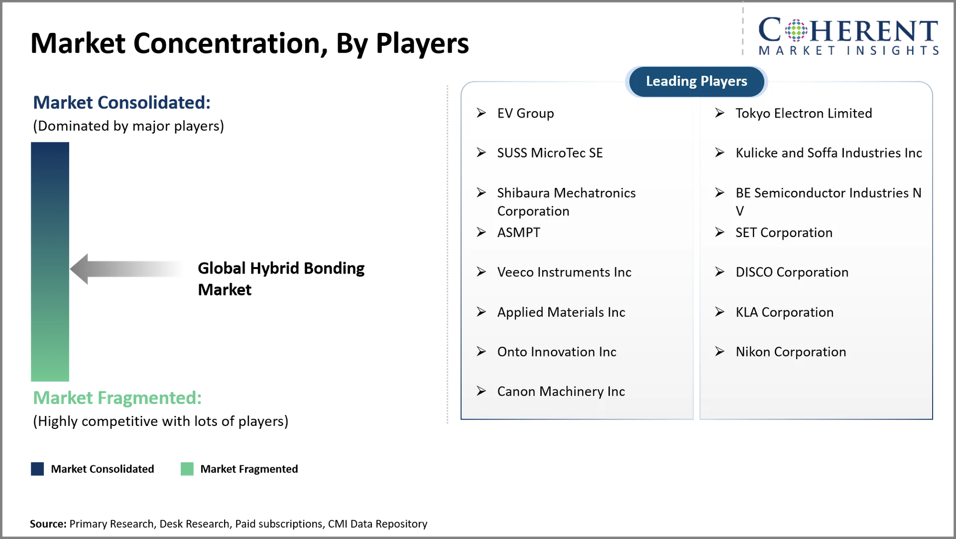
The hybrid bonding landscape is led by TSMC, Intel, Samsung Electronics, SK hynix, and Applied Materials, with strategies increasingly centered on fine-pitch integration and artificial intelligence hardware. TSMC is scaling SoIC, with three-nanometer stacking entering volume production in 2025 and a roadmap toward smaller bonding pitches. Intel is commercializing Foveros Direct for the 3D integration of chiplets, including the Clearwater Forest server processors. SK hynix is eyeing hybrid bonding for future high-bandwidth memory stacks, especially as stack heights and input/output needs rise. Samsung Electronics is pushing ahead with three-dimensional memory and logic integration and bolstering its high-bandwidth memory portfolio. Equipment suppliers are consequently focusing on alignment accuracy, surface preparation, bonding throughput, and nanoscale inspection.
Market Report Scope
Global Hybrid Bonding Market Report Coverage | |||
Report Coverage | Details | ||
Base Year | 2025 | Market Size in 2026: | USD 200.0 Mn |
Historical Data For: | 2020 To 2024 | Forecast Period: | 2026 To 2033 |
Forecast Period 2026 To 2033 CAGR: | 18.00% | 2033 Value Projection: | USD 931.0 Mn |
Geographies covered: |
| ||
Segments covered: |
| ||
Companies covered: | EV Group, Tokyo Electron Limited, SUSS MicroTec SE, Kulicke and Soffa Industries Inc, Shibaura Mechatronics Corporation, BE Semiconductor Industries N V, ASMPT, SET Corporation, Veeco Instruments Inc, DISCO Corporation, Applied Materials Inc, KLA Corporation, Onto Innovation Inc, Nikon Corporation, Canon Machinery Inc | ||
Growth Drivers: |
| ||
Restraints & Challenges: |
| ||
Analyst Opinion (Expert Opinion)
- The future of hybrid bonding will shift from selective three-dimensional logic applications toward broader heterogeneous integration. Logic stacking is already moving into high-volume manufacturing, while memory adoption remains more technically demanding. TSMC and Intel demonstrate that copper-to-copper bonding can support commercial three-dimensional processor architectures. The next transition will depend heavily on thermal management, bonding yield, wafer cleanliness, and increasingly tight pitch requirements. High-bandwidth memory will remain a major long-term catalyst as stacked layers increase and conventional micro bump approaches face physical limitations.
- The largest opportunity should concentrate on wafer-to-wafer and chip-to-wafer bonding for artificial intelligence processors, high-bandwidth memory, and chiplet architectures. Taiwan should remain a priority because TSMC combines advanced logic, SoIC, and high-bandwidth memory integration within its packaging ecosystem. South Korea offers substantial opportunities around Samsung Electronics and SK hynix memory development. The U.S. presents another strong opportunity as Intel expands domestic advanced packaging and SK hynix develops its Indiana high-bandwidth memory packaging facility.
- Players seeking an edge should prioritize sub-five-micrometer alignment, higher bonding throughput, surface-defect detection, and process control. Equipment companies should develop integrated cleaning, activation, alignment, bonding, and inspection platforms rather than isolated tools. Suppliers should also optimize systems for high-bandwidth memory's increasing stack heights and input/output densities. Materials companies can differentiate through lower-temperature bonding and improved wafer-surface compatibility. Partnerships with foundries and memory manufacturers will be particularly important because hybrid bonding qualification requires close integration between equipment, materials, process recipes, and device architectures.
Speak to the analyst
Want personalized insights?
Take the findings above to one of our principal consultants, or have the report rebuilt around the segments, geographies and competitors you actually track.
Market Segmentation
- Bonding Type Insights (Revenue, USD Million, 2021 - 2033)
- Wafer-to-Wafer Bonding
- Die-to-Wafer Bonding
- Die-to-Die Bonding
- Equipment Type Insights (Revenue, USD Million, 2021 - 2033)
- Wafer Bonders
- Die Bonders
- Alignment And Inspection Systems
- Others
- Application Insights (Revenue, USD Million, 2021 - 2033)
- 3D Integrated Circuits
- 5D Integrated Circuits
- High-Bandwidth Memory
- CMOS Image Sensors
- Microelectromechanical Systems
- Advanced Logic Devices
- Memory Devices
- End User Insights (Revenue, USD Million, 2021 - 2033)
- Semiconductor Foundries
- Integrated Device Manufacturers
- Outsourced Semiconductor Assembly and Test Providers
- Research Institutes
- Others
- Regional Insights (Revenue, USD Million, 2021 - 2033)
- North America
- U.S.
- Canada
- Latin America
- Brazil
- Argentina
- Mexico
- Rest of Latin America
- Europe
- Germany
- U.K.
- Spain
- France
- Italy
- Russia
- Rest of Europe
- Asia Pacific
- China
- India
- Japan
- Australia
- South Korea
- ASEAN
- Rest of Asia Pacific
- Middle East
- GCC Countries
- Israel
- Rest of Middle East
- Africa
- South Africa
- North Africa
- Central Africa
- North America
Sources
Primary Research Interviews
- Semiconductor Manufacturers & Foundries
- Advanced Packaging Technology Providers
- Wafer Bonding Equipment Suppliers
- Integrated Device Manufacturers (IDMs)
Magazines
- Semiconductor Digest
- IEEE Spectrum
- Advanced Packaging Magazine
- Solid State Technology
Journals
- Journal of Electronic Materials
- IEEE Transactions on Semiconductor Manufacturing
- Journal of Microelectronics and Electronic Packaging
Associations
- Semiconductor Industry Association (SIA)
- SEMI (Semiconductor Equipment and Materials International)
- International Electronics Manufacturing Initiative (iNEMI)
- European Semiconductor Industry Association (ESIA)
Public Domain Sources
- U.S. International Trade Administration (ITA)
- World Semiconductor Trade Statistics (WSTS)
- National Institute of Standards and Technology (NIST)
- European Commission – Digital Economy Reports
Proprietary Elements
- CMI Data Analytics Tool
- Proprietary CMI Existing Repository of Information for Last 10 Years
Get access to 250+ pages report
Every segment, forecast, competitor profile and data table behind the analysis above — available for instant download.
- ESOMAR Member
- ISO 9001:2015 Certified
- D-U-N-S Registered
- GDPR & CCPA Compliant
Frequently Asked Questions
The global hybrid bonding market is expected to stand at USD 200.0 Mn in 2026 and is expected to reach USD 931.0 Mn by 2033.
The CAGR of the global hybrid bonding market is projected to be 18.0% from 2026 to 2033.
Growing adoption of 3D integrated circuits and advanced semiconductor packaging and Rising demand for high-bandwidth memory architectures are the major factors driving the growth of the global hybrid bonding market.
High capital requirements for hybrid bonding equipment and Complex surface preparation and contamination control requirements are the major factors hampering the growth of the global hybrid bonding market.
In terms of bonding type, wafer-to-wafer bonding segment is estimated to dominate the market revenue share in 2026.
Hybrid bonding is a semiconductor packaging process that directly joins dielectric and metal surfaces between wafers or dies.
Hybrid bonding enables finer interconnect pitches and supports higher-density stacking for advanced high-bandwidth memory architectures.