

Global Hybrid-Bonding Surface Preparation & Bond Interface Inspection Market Size and Forecast – 2026-2033
The global hybrid-bonding surface preparation & bond interface inspection market is expected to grow from USD 0.38 Bn in 2026 to USD 2.45 Bn by 2033, registering a compound annual growth rate (CAGR) of 30.3% from 2026 to 2033. The global hybrid-bonding surface preparation & bond interface inspection market is driven by Growing demand for higher interconnect density in three-dimensional integrated circuits. On May 28, 2026, imec and EV Group (EVG) presented a robust and highly yielding wafer-to-wafer hybrid bonding technology at 200nm Cu interconnect pad pitch, demonstrated on a test vehicle with routable interconnects.
Key Takeaways of the Global Hybrid-Bonding Surface Preparation & Bond Interface Inspection Market
- The Wafer-to-Wafer Hybrid Bonding segment is expected to account for 52.0% of the global hybrid-bonding surface preparation & bond interface inspection market share in 2026. Increasing investments in wafer-to-wafer and die-to-wafer hybrid bonding technologies is driving the growth of the segment. On May 26, 2026, Advanced Semiconductor Engineering announced an automated 310-millimeter by 310-millimeter panel-level packaging production line.
- The Plasma Surface Activation segment is estimated to capture 37.0% of the market share in 2026. Rising need for precise surface cleanliness and nanoscale interface inspection is majorly driving the growth of the segment. On February 18, 2026, Plasmatreat USA announced expanded plasma nozzle and HydroPlasma cleaning technologies. The company highlighted its PDW100 and PFA10 plasma nozzles for semiconductor packaging applications.
- The Optical Inspection segment is estimated to capture 33.0% of the market share in 2026. Growing semiconductor industry investments in heterogeneous integration and chiplet architectures is majorly driving the growth of the segment. On May 21, 2026, Advanced Micro Devices announced investments exceeding USD 10 billion across Taiwan's semiconductor ecosystem.
- Asia Pacific is expected to dominate the hybrid-bonding surface preparation & bond interface inspection market in 2026 with a market share of 43.0%. Expansion of hybrid bonding applications in high-bandwidth memory manufacturing in Asia Pacific is driving the growth of the regional market. On July 23, 2025, Hanmi Semiconductor signed a technology development agreement with TES. The collaboration combines Hanmi's precision bonding expertise with TES's plasma processing, thin-film deposition, and cleaning technologies.
- North America is expected to account for 29.0% share in 2026 and is projected to record the fastest growth over the forecast period. Development of AI-powered defect detection systems in North America is driving the growth of the regional market. On February 19, 2025, Applied Materials introduced its SEMVision H20 defect review system. The platform combines cold field emission electron-beam imaging with deep-learning artificial intelligence models.
Segmental Insights
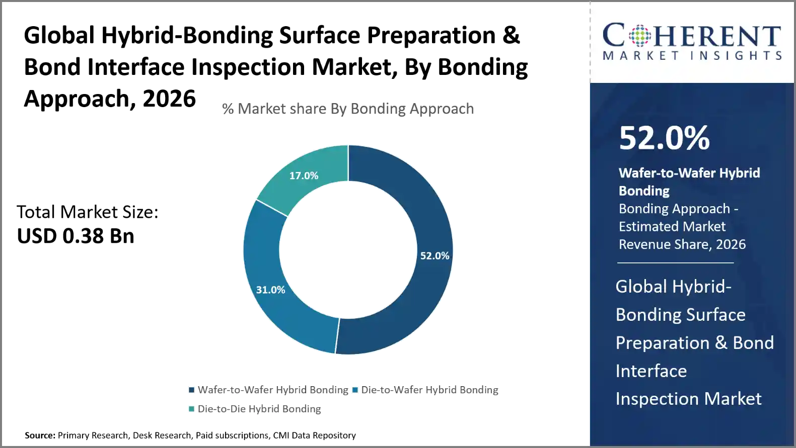
Why Does Wafer-to-Wafer Hybrid Bonding Dominate the Global Hybrid-Bonding Surface Preparation & Bond Interface Inspection Market?
The wafer-to-wafer hybrid bonding segment is expected to account for 52.0% of the global hybrid-bonding surface preparation & bond interface inspection market share in 2026. The wafer-to-wafer hybrid bonding is the most used approach, since it allows the simultaneous connection of whole semiconductor wafers. The method enables high-density connectivity and uniform alignment on vast bonding regions. It eliminates individual die placement requirements and allows for cost-effective manufacturing of vertically integrated devices. The technique is particularly relevant to image sensors, memory stacks and advanced three-dimensional integrated circuits. Uniform surface preparation, precise planarization, and wafer-level inspection continue to be important for bonding yield. These advantages strengthen demand for specialized wafer cleaning, surface activation, and bond interface inspection equipment.
On November 12, 2025, Tower Semiconductor announced the expansion of its existing, mature 300mm wafer bonding technology, originally developed and in mass production for stacked BSI image sensors, to enable heterogeneous 3D-IC integration across its industry-leading Silicon Photonics (SiPho) and SiGe BiCMOS processes, including full support by Cadence design tools for the stacked platform technology.
- Current Industry Events of 2026
- Market Size Estimation
- Regional Breakdown
- Competitive Landscape
- Customer Intelligence
- Segmental Analysis
- Pricing Analysis
- Key Market Drivers, Challenges & Future Trends
- Customized Insights Section
Why is Plasma Surface Activation the Most Crucial Surface Preparation Technology?
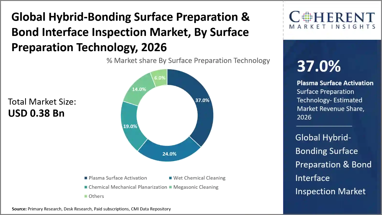
The plasma surface activation segment is expected to account for 37.0% of the global hybrid-bonding surface preparation & bond interface inspection market share in 2026. The importance of plasma surface activation is that it increases the surface reactivity and improves the dielectric-to-dielectric and copper-to-copper bonding. The treatment alters surface chemistry, enhances wettability and cleans residual organic contaminants. It enables hydrophilic bonding by introducing reactive surface groups to form stronger interfacial bonds. Plasma activation also allows bonding at lower temperatures and reduces interfacial void formation. Different plasma chemistries are used to meet specific material needs. These qualities are required for reliable fine-pitch interconnections as well as consistent hybrid bonding quality, hence plasma activation is a must-have process.
On September 30, 2025, Tokyo Electron gave an update on advanced packaging technology, outlining its Synapse Si wafer-bonding device. The platform combines plasma control, cleaning, and high-precision alignment. Its process technologies support copper hybrid bonding and fusion bonding.
Optical Inspection Dominates the Global Hybrid-Bonding Surface Preparation & Bond Interface Inspection Market
The optical inspection segment is expected to account for 33.0% of the global hybrid-bonding surface preparation & bond interface inspection market share in 2026. Optical inspection dominates because it enables rapid, non-contact examination of wafer surfaces throughout hybrid bonding manufacturing. The system can detect particles, scratches, surface contaminants, misalignments and obvious bonding faults. High-resolution imaging allows for accurate evaluation of surface conditions before wafers are loaded into bonding equipment. Optical inspection also allows for automated wafer mapping and repeatable flaw identification across production batches. Infrared optical imaging provides improved inspection capability by detecting subsurface cavities and analyzing concealed bonding connections. It can be compatible with automated manufacturing lines, which allows for high-throughput quality monitoring and decreases the chance of defective semiconductor assemblies.
On February 18, 2025, TASMIT introduced its INSPECTRA System for Advanced semiconductor packaging. Polarized-light optical inspection detects particles, pattern faults, cracks and interior defects. The platform observes both the surfaces of the substrate and its interior structures.
Current Events and their Impact
Current Events | Description and its Impact |
European Union Chips Act, Regulation (EU) 2023/1781 |
|
European Union Fluorinated Greenhouse Gases Regulation, Regulation (EU) 2024/573 |
|
Hybrid-Bonding Surface Preparation & Bond Interface Inspection Market Dynamics
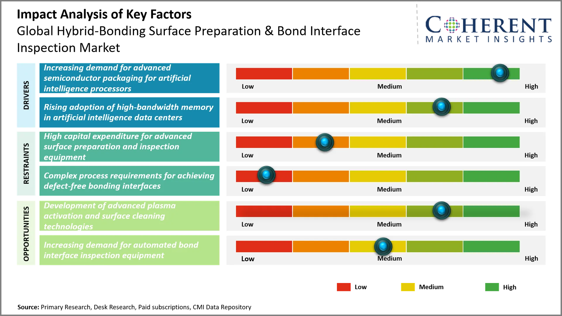
Market Drivers
Increasing demand for advanced semiconductor packaging for artificial intelligence processors
The increasing workload of artificial intelligence is boosting the demand for advanced semiconductor packaging technologies that improve the performance and integration density of processors. AI processors demand faster connectivity between computer units, memory components and specialized accelerators. Hybrid bonding offers direct copper-to-copper connections with ultra-fine connector pitches and lower electrical resistance. This architecture enables chiplet integration and 3D stacking while boosting bandwidth and power efficiency. There is a growing need for accurate wafer planarization, plasma activation and contaminant removal prior to bonding among manufacturers. Advanced optical inspection and interface metrology can detect alignment faults, particulates and bonding defects. These restrictions are driving the demand for specialist surface prep and inspection equipment.
On June 4, 2025, GlobalFoundries announced plans to invest USD 16 billion to develop its semiconductor manufacturing and advanced packaging capabilities across its New York and Vermont plants. GF’s investment is a deliberate response to growing growth in AI that is accelerating demand for next-generation semiconductors built for power efficiency and high-bandwidth performance.
Rising adoption of high-bandwidth memory in artificial intelligence data centers
Increasing deployment of high-bandwidth memory in artificial intelligence data centers is driving demand for improved wafer stacking technologies. High-bandwidth memory connects many vertically stacked memory dies to a specialized logic die. Hybrid bonding allows for finer linkages and shorter electrical paths than typical microbump-based interconnections. The architecture offers higher memory bandwidth, improved signal integrity and increased integration density. To ensure reliable stacking, semiconductor producers demand highly homogeneous wafer surfaces and accurate alignment of copper pads. The plasma activation and improved cleaning techniques enhance the bonding conditions and the interfacial strength. Bonding flaws and interior voids can be detected using optical and infrared inspection technology. These manufacturing requirements provide opportunity for specialized surface preparation and bond interface inspection equipment.
On March 19, 2025, SK hynix announced it has shipped its next-generation HBM4 memory to major customers. The 12-layer samples provided more bandwidth and capacity for artificial intelligence processors. Customer certification was planned ahead to the bulk manufacturing.
Emerging Trends
- Increasing adoption of hybrid bonding for advanced chiplet integration: Semiconductor manufacturers are increasingly adopting hybrid bonding to integrate chiplets, which provides a finer interconnection, higher packaging density and improved electrical performance for advanced computing architectures.
- Impact: This change increases demands on accurate wafer planarization, plasma activation, particle removal, and advanced inspection systems to ensure dependable bonding interfaces and manufacturing yields.
- Relevance to the market: TSMC's SoIC technology solidifies this trend through three-dimensional chip integration, creating demand for specialized surface preparation and interface inspection solutions.
- Development of advanced inspection technologies for buried bonding interfaces: Equipment manufacturers are pushing infrared imaging, acoustic inspection and automated defect detection to find hidden voids and bonding irregularities within stacked semiconductor structures.
- Impact: These technologies enhance defect detection, increase production quality control and lower the danger of undetected interface failures in modern semiconductor packaging processes.
- Relevance to the market: Infrared inspection of bonded wafer stacks creates opportunities for specialized metrology suppliers supporting high-bandwidth memory and three-dimensional integrated circuit production.
Regional Insights
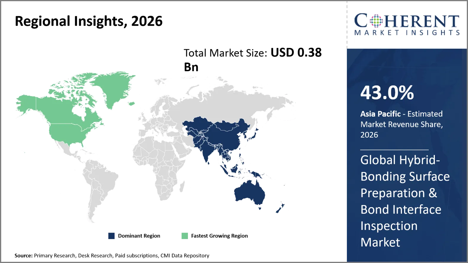
Why is Asia Pacific a Strong Market for Hybrid-Bonding Surface Preparation & Bond Interface Inspection?
Asia Pacific is expected to account for a market share of 43.0% in 2026. Asia Pacific benefits from expanding outsourced semiconductor assembly and testing operations and cross-border advanced packaging investments. Chipbond Technology has opened a new manufacturing plant in Penang in February 2026, as Malaysia builds its packaging ecosystem. Polymatech Electronics is establishing an advanced manufacturing facility, injecting specialist electronics packaging capital into Singapore. Such trends are forcing regional providers to bring wafer cleaning, surface conditioning and automated inspection capabilities to market. Regional manufacturing diversification is creating opportunities for equipment suppliers serving multiple packaging facilities. Growing collaboration between semiconductor manufacturers and local equipment companies further supports specialized hybrid-bonding process development.
Why Does North America Hybrid-Bonding Surface Preparation & Bond Interface Inspection Market Exhibit High Growth?
North America is expected to register the fastest growth with a CAGR of 31.1% over the forecast period. North America is projected to account for 29.0% of the global hybrid-bonding surface preparation & bond interface inspection market in 2026. North America is experiencing growing demand for hybrid-bonding inspection technologies because semiconductor manufacturers require more reliable methods for qualifying heterogeneous packaging processes. For example, the National Institute of Standards and Technology is developing metrology methods for predicting bonding quality based on pretreated surface measurements. Its research focuses on surface characterization and process repeatability for advanced packaging applications. Planarity, surface roughness, nano topography, and alignment are other key metrology needs as stated in the International Roadmap for Devices and Systems. These efforts are meant to motivate the equipment manufacturers to enhance the measurement accuracy and to establish rational inspection methods for complex bonded semiconductor devices.
Global Hybrid-Bonding Surface Preparation & Bond Interface Inspection Market Outlook for Key Countries
Why is China Emerging as a Major Hub in the Hybrid-Bonding Surface Preparation & Bond Interface Inspection Market?
China is aiming to enhance its local hybrid-bonding equipment capability through local development of integrated solutions for wafer preparation and bonding. Beijing U-Precision Technology offers automated wafer bonding equipment with plasma activation, surface cleaning, precision alignment, and alignment verification. It has an integrated design comprising a number of core steps of wafer-to-wafer hybrid bonding. Another advancement came in a procurement project in December 2025 by the Xi'an Flight Automatic Control Research Institute. The tender was for die-to-wafer bonding equipment including plasma activation, wafer cleaning, alignment, bonding and fault detection. These procurement actions reflect increased domestic demand in specialized bonding infrastructure and localized inspection capabilities.
Is U.S. the Next Growth Engine for the Hybrid-Bonding Surface Preparation & Bond Interface Inspection Market?
The U.S. market benefits from commercial development of integrated hybrid-bonding platforms for artificial intelligence and high-performance computing applications. Applied Materials introduced its Kinex platform with integrated wet cleaning, plasma activation, infrared metrology, and die-to-wafer bonding. The platform uses technologies developed with BE Semiconductor Industries. Its integrated architecture decreases the chance of contamination between essential processing steps and offers more constant bonding conditions. The National Institute of Standards and Technology is also looking on nanoscale mechanical characterization utilizing multimodal atomic force microscopy. These developments strengthen demand for integrated preparation systems and advanced interface characterization equipment.
Taiwan Hybrid-Bonding Surface Preparation & Bond Interface Inspection Market Analysis and Trends
Taiwan benefits from its advanced foundry ecosystem and growing development of dedicated hybrid-bonding production equipment. The SUSS MicroTec XBC300 Gen2 platform offers die-to-wafer bonding, wafer-to-wafer bonding and surface preparation. Its surface preparation cluster includes plasma activation, aqueous cleaning and infrared void detection. The platform also enables in-situ metrology and semiconductor grade cleaning requirements. Seiki Semiconductor has announced the launch of its 82CWW dual-mode hybrid-bonding system at SEMICON Taiwan 2025. The equipment handles 200 mm and 300 mm wafers including ultra-thin substrates down to 35 micrometers. These advances fuel the local demand for precision surface conditioning and bonding inspection technology.
Japan Hybrid-Bonding Surface Preparation & Bond Interface Inspection Market Analysis and Trends
Japan has a mature semiconductor materials and equipment sector, especially in chemical mechanical planarization and plasma-based surface treatment. FUJIFILM Corporation announced the launch of a high-end packaging CMP slurry dedicated to hybrid-bonding applications in September 2025. The product was adopted by a major semiconductor manufacturer for planarizing bonding surfaces. ULVAC is also developing dedicated plasma activation technologies for die-to-wafer bonding. Its process combines gentle plasma treatment, vacuum-based surface protection, and individual-chip processing capabilities. These innovations will enhance Japan’s position in specialized polishing materials, surface activation equipment and technology for preparing wafers under conditions of contamination control.
South Korea Hybrid-Bonding Surface Preparation & Bond Interface Inspection Market Analysis and Trends
South Korea benefits from semiconductor memory manufacturers' development of next-generation wafer stacking and hybrid-bonded memory architectures. Samsung Electronics is evaluating non-destructive inspection technologies for identifying microscopic voids within bonded semiconductor interfaces. Onto Innovation's picosecond laser ultrasound technology represents an emerging solution for examining buried bonding defects. Separately, South Korea's Ministry of Trade, Industry and Resources is supporting international standardization of semiconductor packaging processes. Korean proposals include standardized methods for evaluating hybrid-bonding strength and wafer dicing precision. These developments strengthen demand for specialized inspection equipment, bonding reliability assessment, and standardized interface quality verification.
Global Hybrid-Bonding Surface Preparation & Bond Interface Inspection Market - Hybrid Bonding Equipment Installation Announcements (2025-2026)
Announcement Date | Company/Customer | Equipment / Platform | Location | Bonding Mode |
December 16, 2025 | NHanced Semiconductors / BE Semiconductor Industries | Datacon 8800 CHAMEO ultra plus | Morrisville, U.S. | Die-to-wafer |
May 26, 2025 | SUSS MicroTec / SET Corporation | XBC300 Gen2 D2W | Sternenfels, Germany | Die-to-wafer |
September 2025 | Seiki Semiconductor | 82CWW Series | Taiwan | Wafer-to-wafer and die-to-wafer |
February 25, 2026 | Hanwha Semitech | SHB2 Nano | South Korea | Die-to-wafer |
May 28, 2026 | EV Group / imec | GEMINI FB | imec, Belgium | Wafer-to-wafer |
How is Development of Advanced Plasma Activation and Surface Cleaning Technologies Creating New Growth Opportunities in the Hybrid-Bonding Surface Preparation & Bond Interface Inspection Market?
Development of advanced plasma activation and surface cleaning technologies is creating opportunities through improved copper surface protection and controlled dielectric preparation before hybrid bonding. ULVAC’s atmospheric-pressure plasma technology enables localized surface treatment without conventional vacuum processing. This method provides equipment engineers with chances to simplify the chip level preparation and lower the complexity of processing. FUJIFILM Corporation's advanced packaging chemical mechanical planarization slurry also meets the surface uniformity criteria for hybrid-bonding applications. Such improvements motivate vendors to develop application specific cleaning chemistries, selective plasma treatments and integrated surface certification systems. Equipment makers can differentiate their products by improving copper oxidation control and reducing surface contamination.
On February 5, 2026, ASMPT announced that it obtained a follow-on order for two ultrafine pitch Thermo-Compression Bonding (TCB) equipment with ASMPT’s unique plasma Active Oxide Removal (AOR) technology from a key client for C2W applications. This strengthens ASMPT’s strategic position as a leading and holistic semiconductor solutions provider with exceptional technology.
Market Players, Key Development, and Competitive Landscape
Key Developments
- On October 31, 2025, SCREEN Holdings Co., Ltd. announced the acquisition of an R&D business in wafer bonding from Nikon Corporation. The latest acquisition will allow SCREEN Holdings to combine Nikon's ultra-high-precision bonding technology with its proprietary technology as the company seeks to lead the world in bonding technology and establish a presence in this field.
- On September 25, 2025, KOKUSAI ELECTRIC CORPORATION entered into a joint development agreement with ASMPT Limited, which provides hardware and software solutions for semiconductor and SMT manufacturing, regarding hybrid bonding and TCB bonding in semiconductor packaging technology.
- On April 7, 2025, HORIBA STEC KOREA, Ltd., a HORIBA subsidiary, acquired EtaMax Co., Ltd., a developer, manufacturer, and seller of wafer inspection system for the semiconductor market. The share transfer was completed on April 3, 2025. The HORIBA Group aims to expand its lineup of wafer inspection system and enhance its solution-proposal capabilities by integrating spectroscopy-related technologies.
Competitive Landscape
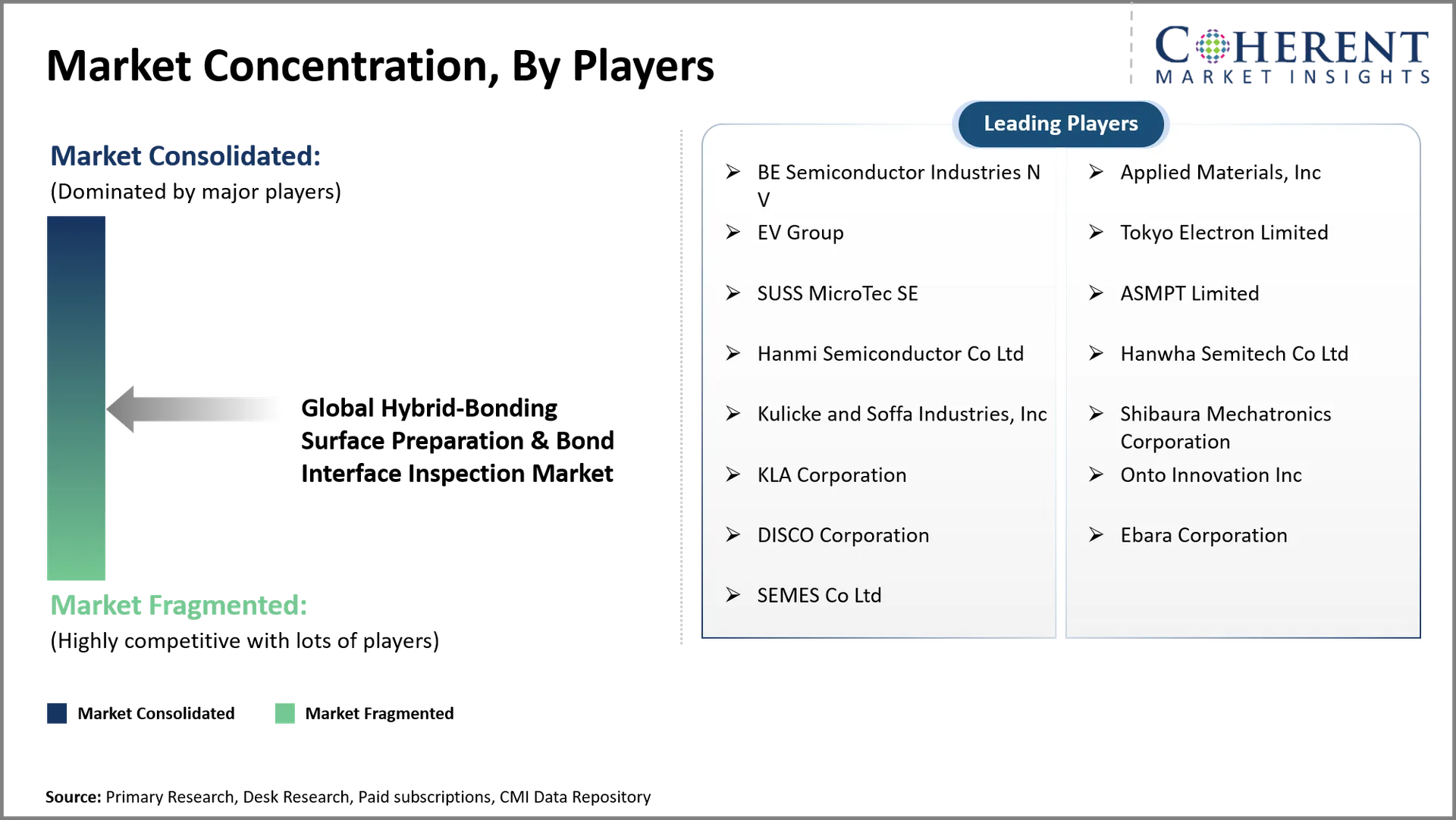
The competitive landscape is led by Applied Materials, BE Semiconductor Industries, EV Group, and SUSS MicroTec. Applied Materials is strengthening its position further with process engineering integration and its Kinex hybrid-bonding platform it created with BE Semiconductor Industries. Kinex combines wet cleaning, plasma activation, infrared metrology and precise bonding in one system. BE Semiconductor Industries has improved die-placement precision and assembly expertise. EV Group is a specialist in wafer bonding, surface activation, cleaning and alignment solutions for advanced semiconductor integration. SUSS MicroTec is increasing its XBC300 Gen2 line for wafer-to-wafer and die-to-wafer bonding applications. Other key players include Tokyo Electron, Shibaura Mechatronics, Onto Innovation and KLA Corporation. Their competitive strategies emphasize process integration, defect detection, contamination control, and precision metrology.
Top Manufacturers and Notable Products in the Hybrid-Bonding Surface Preparation & Bond Interface Inspection Market
Manufacturer | Notable Product | Key features |
EV Group | GEMINI FB | Sub-50 nm alignment, integrated cleaning, low-temperature plasma activation, alignment verification, modular processing |
Applied Materials | Kinex Bonding System | Integrated bonding process, high-accuracy die placement, controlled processing environment, in-line metrology, overlay drift detection |
BE Semiconductor Industries | Datacon 8800 CHAMEO ultra plus | 100 nm alignment accuracy, ISO 3 working environment, in-line infrared inspection, up to 2000 components per hour |
SUSS MicroTec | XBC300 Gen2 D2W/W2W | Below 100 nm wafer-to-wafer alignment, integrated in-situ metrology, 200 mm and 300 mm substrate compatibility, integrated cleaning modules |
Tokyo Electron | Synapse Si | 300 mm wafer compatibility, three-sigma alignment accuracy below 100 nm, high-reliability bonding, production-oriented wafer processing |
Market Report Scope
Analyst Opinion (Expert Opinion)
- The future of this industry will increasingly depend on controlling surface conditions before bonding and verifying buried interfaces afterward. Hybrid bonding will become particularly important for advanced logic, chiplet integration, and vertically stacked memory architectures. Equipment suppliers should prioritize integrated preparation systems combining chemical mechanical planarization, plasma activation, precision cleaning, and infrared inspection. The strongest competitive advantage will come from maintaining consistent surface quality across multiple bonding stages. Suppliers capable of reducing contamination exposure and identifying microscopic interface defects will attract greater interest from advanced packaging manufacturers.
- The maximum opportunity will emerge in die-to-wafer preparation and inspection for artificial intelligence processors and heterogeneous chiplet architectures. Taiwan is especially desirable since TSMC’s System on Integrated Chips technology demands flawless wafer and die integration. Another possible potential is South Korea through the development of enhanced memory stacking and hybrid-bonding. There are potential for the U.S. in high-performance computer packaging and in domestic semiconductor equipment development. The focus for manufacturers should be on infrared void detection, automated surface qualifying, and precision alignment verification. These applications need custom inspection solutions, not the generic wafer defect detection tools.
- Market participants must create collaborative programs with foundries, outsourced semiconductor assembly and test providers and integrated device manufacturers. Equipment suppliers should build modular platforms to address wafer-to-wafer and die-to-wafer preparation needs. They should also enhance compatibility between cleaning chemistries, plasma activation recipes and copper surface protection methods. The inspection specialist focus should be on buried interface characterization and automated defect classification. Companies having application engineering teams in Taiwan, South Korea, Japan and the U.S. may respond more quickly to customer certification requirements. Strategic partnerships with bonding equipment manufacturers can also strengthen technology adoption and customer retention.
Speak to the analyst
Want personalized insights?
Take the findings above to one of our principal consultants, or have the report rebuilt around the segments, geographies and competitors you actually track.
Market Segmentation
- Bonding Approach Insights (Revenue, USD Billion, 2021 - 2033)
- Wafer-to-Wafer Hybrid Bonding
- Die-to-Wafer Hybrid Bonding
- Die-to-Die Hybrid Bonding
- Surface Preparation Technology Insights (Revenue, USD Billion, 2021 - 2033)
- Plasma Surface Activation
- Wet Chemical Cleaning
- Chemical Mechanical Planarization
- Megasonic Cleaning
- Others
- Inspection Technology Insights (Revenue, USD Billion, 2021 - 2033)
- Optical Inspection
- Infrared Inspection
- Acoustic Inspection
- Scanning Electron Microscopy
- Atomic Force Microscopy
- Surface Topography Inspection
- Defect and Void Inspection
- Equipment Type Insights (Revenue, USD Billion, 2021 - 2033)
- Surface Preparation Equipment
- Plasma Activation Systems
- Wafer Cleaning Systems
- Chemical Mechanical Planarization Equipment
- Bond Interface Inspection Equipment
- Others
- Application Insights (Revenue, USD Billion, 2021 - 2033)
- High-Bandwidth Memory
- Three-Dimensional Integrated Circuits
- Artificial Intelligence Processors
- High-Performance Computing
- Advanced Logic Devices
- CMOS Image Sensors
- Chiplet-Based Semiconductor Devices
- End User Insights (Revenue, USD Billion, 2021 - 2033)
- Integrated Device Manufacturers
- Semiconductor Foundries
- Outsourced Semiconductor Assembly and Test Providers
- Memory Manufacturers
- Research and Development Facilities
- Regional Insights (Revenue, USD Billion, 2021 - 2033)
- North America
- U.S.
- Canada
- Latin America
- Brazil
- Argentina
- Mexico
- Rest of Latin America
- Europe
- Germany
- U.K.
- Spain
- France
- Italy
- Russia
- Rest of Europe
- Asia Pacific
- China
- India
- Japan
- Australia
- South Korea
- ASEAN
- Rest of Asia Pacific
- Middle East
- GCC Countries
- Israel
- Rest of Middle East
- Africa
- South Africa
- North Africa
- Central Africa
- North America
- Key Players Insights
- BE Semiconductor Industries N V
- Applied Materials, Inc
- EV Group
- Tokyo Electron Limited
- SUSS MicroTec SE
- ASMPT Limited
- Hanmi Semiconductor Co Ltd
- Hanwha Semitech Co Ltd
- Kulicke and Soffa Industries, Inc
- Shibaura Mechatronics Corporation
- KLA Corporation
- Onto Innovation Inc
- DISCO Corporation
- Ebara Corporation
- SEMES Co Ltd
Sources
Primary Research Interviews
- Semiconductor Equipment Manufacturers
- Wafer Bonding Technology Specialists
- Advanced Packaging Engineers & Process Technologists
- Metrology & Inspection Solution Providers
Magazines
- Semiconductor Digest
- Advanced Packaging Magazine
- Solid State Technology
- IEEE Spectrum
Journals
- Journal of Electronic Materials (Springer)
- IEEE Transactions on Semiconductor Manufacturing
- Journal of Vacuum Science & Technology
Associations
- SEMI (Semiconductor Equipment and Materials International)
- IEEE Electron Devices Society
- International Wafer-Level Packaging Conference (IWLPC)
- IMAPS (International Microelectronics Assembly and Packaging Society)
Public Domain Sources
- U.S. Semiconductor Industry Association (SIA) Reports
- NIST (National Institute of Standards and Technology) Publications
- European Semiconductor Industry Association (ESIA) Reports
- IRDS (International Roadmap for Devices and Systems) Publications
Proprietary Elements
- CMI Data Analytics Tool
- Proprietary CMI Existing Repository of information for last 10 years
Get access to 250+ pages report
Every segment, forecast, competitor profile and data table behind the analysis above — available for instant download.
- ESOMAR Member
- ISO 9001:2015 Certified
- D-U-N-S Registered
- GDPR & CCPA Compliant
Frequently Asked Questions
The global hybrid-bonding surface preparation & bond interface inspection market is expected to stand at USD 0.38 Bn in 2026 and is expected to reach USD 2.45 Bn by 2033.
The CAGR of the global hybrid-bonding surface preparation & bond interface inspection market is projected to be 30.3% from 2026 to 2033.
Increasing demand for advanced semiconductor packaging for artificial intelligence processors and Rising adoption of high-bandwidth memory in artificial intelligence data centers are the major factors driving the growth of the global hybrid-bonding surface preparation & bond interface inspection market.
High capital expenditure for advanced surface preparation and inspection equipment and Complex process requirements for achieving defect-free bonding interfaces are the major factors hampering the growth of the global hybrid-bonding surface preparation & bond interface inspection market.
In terms of bonding approach, wafer-to-wafer hybrid bonding segment is estimated to dominate the market revenue share in 2026.
This market covers equipment, materials, and technologies used to prepare semiconductor surfaces and inspect bonded interfaces.
Hybrid bonding is an advanced packaging technique that directly connects copper pads and dielectric surfaces without conventional solder microbumps.