

Global Semiconductor Metrology Equipment Market Forecast – 2026 To 2033
The global semiconductor metrology equipment market is expected to grow from USD 16.00 Bn in 2026 to USD 27.00 Bn by 2033, registering a compound annual growth rate (CAGR) of 9.6% from 2026 to 2033. The global semiconductor metrology equipment market is driven by growing use of Extreme Ultraviolet (EUV) lithography. On September 8, 2026, Samsung Electronics and ASML announced an expansion of their long-standing strategic partnership, deepening collaboration on High NA EUV lithography and advanced semiconductor manufacturing technologies that will help drive the next generation of innovation in the AI era.
Key Takeaways of the Global Semiconductor Metrology Equipment Market
- The Optical Systems segment is expected to account for 69.0% of the global semiconductor metrology equipment market share in 2026. Increasing demand for defect detection is driving the growth of the segment. In February 2025, Applied Materials introduced the SEMVision H20 defect review system. The system combines cold field emission electron-beam technology with artificial intelligence image recognition.
- The 2D Metrology and Inspection segment is estimated to capture 46.0% of the market share in 2026. Expansion of advanced semiconductor packaging is majorly driving the growth of the segment. On October 6, 2025, Amkor Technology, Inc. announced an expanded planned investment of its new state-of-the-art outsourced semiconductor advanced packaging and test campus in Arizona, U.S.
- The Wafer Inspection Systems segment is estimated to capture 35.0% of the market share in 2026. Rising use of 3D NAND structures is majorly driving the growth of the segment. In August 2025, SK hynix completed development and began mass production of its 321-layer 2-terabit QLC NAND. The architecture uses expanded planes to combine high capacity with performance.
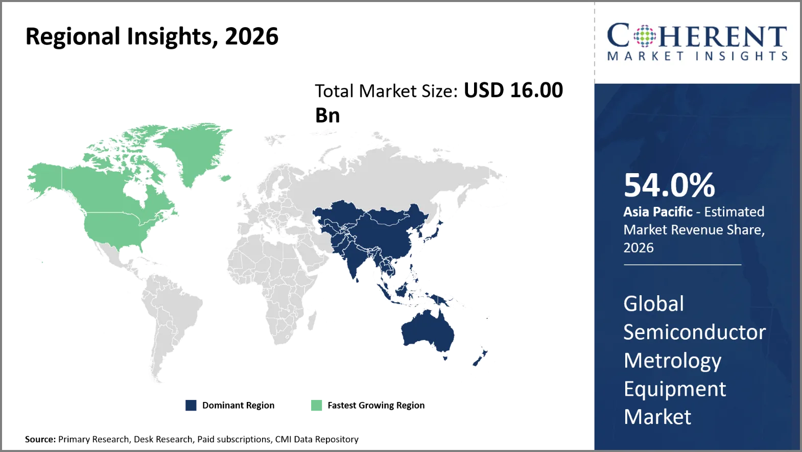
- Asia Pacific is expected to dominate the semiconductor metrology equipment market in 2026 with a market share of 54.0%. Adoption of 3D inspection technologies in Asia Pacific is driving the growth of the regional market. In July 2026, ZEISS Semiconductor Manufacturing Technology opened an Innovation Center in Yongin, South Korea. The facility includes the NLX-100 3D X-ray metrology and inspection system.
- North America is expected to account for 23.0% share in 2026 and is projected to record the fastest growth over the forecast period. Increasing semiconductor fab investments in North America is driving the growth of the regional market. In March 2025, Taiwan Semiconductor Manufacturing Company announced an additional USD 100 billion U.S. investment. The expansion raises planned U.S. investment to USD 165 billion.
Segmental Insights
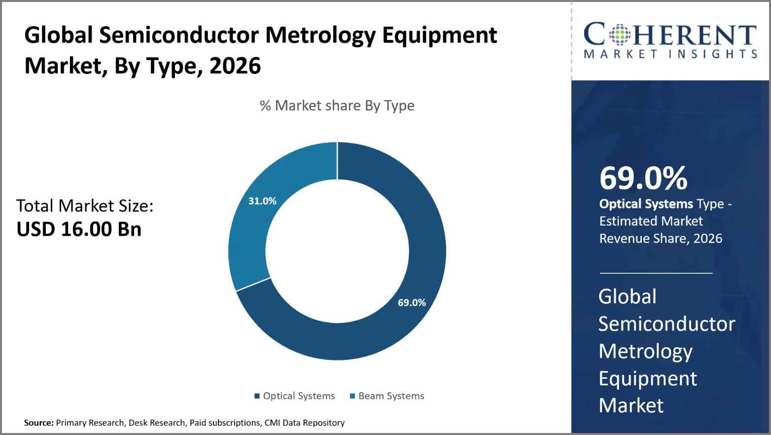
Why Does Optical Systems Dominate the Global Semiconductor Metrology Equipment Market?
The optical systems segment is expected to account for 69.0% of the global semiconductor metrology equipment market share in 2026. Optical systems are dominant as they can measure quickly, accurately and over a large area of the wafer. Many process steps require repeated measurements for the semiconductor producers. Optical devices allow for fast measurements over broad wafer areas. They provide high sensitivity measurements of overlay, crucial dimensions, focus, and pattern features. These features enable ongoing tracking of processes in high volume manufacturing. Optical platforms also lend themselves quite well to automated process-control systems. Their measurement data enables producers to swiftly identify process drift and remedy manufacturing discrepancies. Artificial intelligence also further increases defect categorization and measurement analysis.
On September 9, 2025, Onto Innovation Inc. announced the launch of Atlas G6 optical critical dimension (OCD) metrology system on September 9, 2025, which is designed to meet the increasing complexity of process control for advanced semiconductor nodes. As the industry advances to second generation gate-all-around (GAA) logic and future vertical gate DRAM architectures to power AI applications, manufacturers are facing even tighter structural dimensions, reducing by as much as 30% per generation.
- Current Industry Events of 2026
- Market Size Estimation
- Regional Breakdown
- Competitive Landscape
- Customer Intelligence
- Segmental Analysis
- Pricing Analysis
- Key Market Drivers, Challenges & Future Trends
- Customized Insights Section
Why is 2D Metrology and Inspection the Most Crucial Dimension?
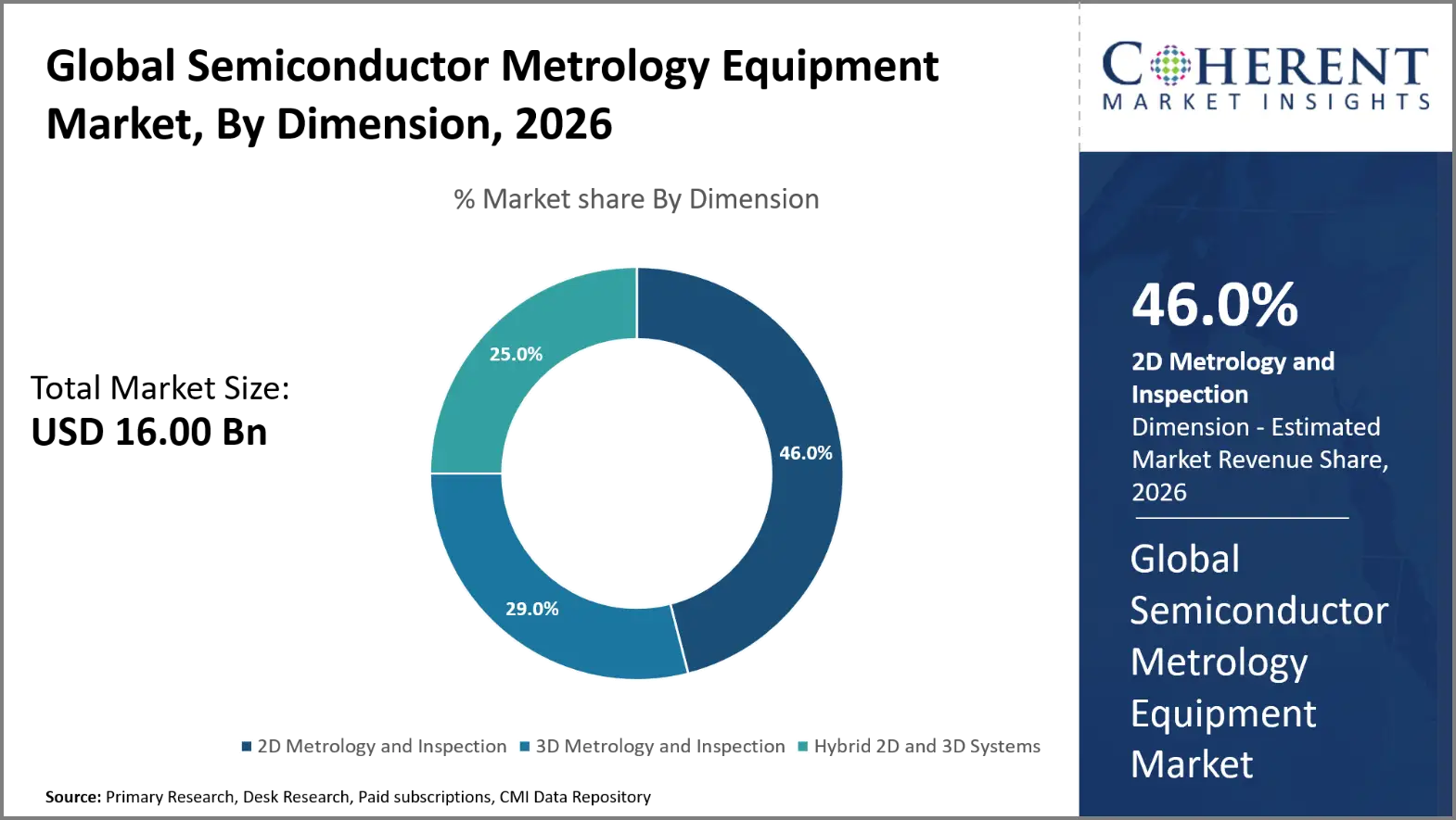
The 2D metrology and Inspection segment is expected to account for 46.0% of the global semiconductor metrology equipment market share in 2026. Lateral pattern precision is critical in semiconductor manufacturing; hence 2D metrology and inspection remain vital. Fabricated structures are designed for critical dimensions for a specific use. Overlay is used to ensure that each succeeding layer of semiconductors is properly aligned. Even little variations in dimensions or alignment might negatively affect device function and manufacturing yield. Advanced lithography technologies demand a more exact control of these parameters. Two-dimensional inspection also detects particles, pattern errors, scratches, and process-related defects on wafer surfaces. In October 2025, Applied Materials launched PROVision 10 for advanced logic and memory metrology. The system provides sub-nanometer imaging for critical-dimension and overlay measurements. Its cold field emission technology increases image resolution by up to 50%. Imaging speed can reach ten times that of conventional thermal field emission systems.
Wafer Inspection Systems Dominates the Global Semiconductor Metrology Equipment Market
The wafer inspection systems segment is expected to account for 35.0% of the global semiconductor metrology equipment market share in 2026. Wafer inspection systems dominate as semiconductor manufacturers must detect defects before they significantly affect production yield. Inspection systems monitor the wafer surface during lithography, etching, depositing and chemical mechanical planarization. They detect particles, scratches, pattern errors and other anomalies in the process. Early diagnosis of defects allows the manufacturer to identify process excursions and take corrective actions. The optical inspection system can inspect a big area of wafer at a high speed. This characteristic makes them particularly useful for high-volume semiconductor manufacturing environments. Advanced transistor designs need more complex topologies and manufacturing methods, which in turn require more inspection.
On September 30, 2026, Hitachi High-Tech Corporation announced it will enhance the development framework for next-generation multi-beam inspection tools in semiconductor manufacturing that is jointly developed with ZEISS Semiconductor Manufacturing Technology. This will accelerate the development of products that enable high-throughput inspections of small defects, which are expected to increase due to further semiconductor device scaling and the adoption of High-NA-EUV lithography.
Current Events and their Impact
Current Events | Description and its Impact |
U.S. - Export Controls on Semiconductor Manufacturing Equipment |
|
European Union Chips Act |
|
Semiconductor Metrology Equipment Market Dynamics
Market Drivers
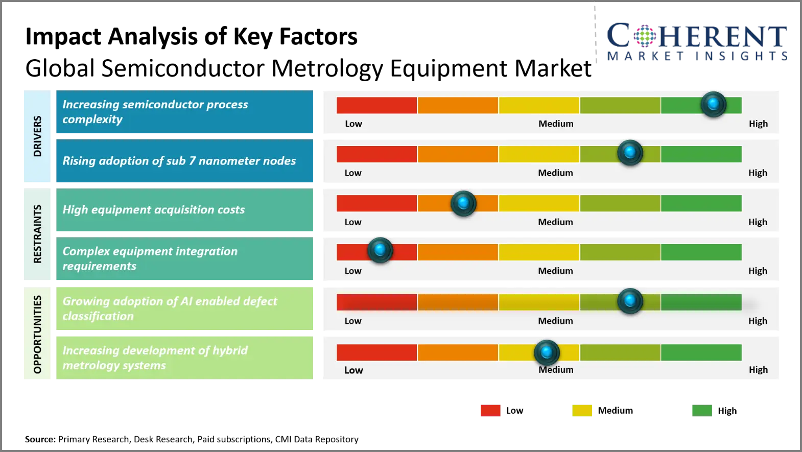
- Increasing semiconductor process complexity: Semiconductor processes are getting more complex as manufacturers are moving toward 3D transistor topologies, enhanced memory architectures and sophisticated packaging designs. Gate-all-around transistors have additional surfaces that need to be measured accurately for dimensions and structure. High-bandwidth memory production also involves multiple stacked dies and demanding bonding processes. These manufacturing changes increase the number of parameters requiring continuous inspection and measurement. Advanced fabs consequently require higher-resolution metrology systems with greater sensitivity and measurement throughput. Process complexity also increases the need for integrated data analysis and automated defect classification.
- On June 16, 2026, At the 2026 IEEE/JSAP Symposium on VLSI Technology & Circuits, Intel Foundry presented progress on a number of important aspects of its front-end silicon process innovations. This includes Intel 18A-P featuring Power Boost, Intel’s first performance enhancement to the 18A node family, now in risk production.
- Rising adoption of sub 7 nanometer nodes: The adoption of sub 7 nanometer semiconductor nodes is increasing demand for highly precise metrology and inspection capabilities. Smaller process dimensions significantly reduce manufacturing tolerances across critical semiconductor structures. Small differences in essential dimensions or overlay can impact the performance and manufacturing yield of the transistors. Advanced nodes also have sophisticated layouts such as gate-all-around transistors and backside power delivery schemes. Such technologies need more detailed measurement at several phases of manufacture. Taiwan Semiconductor Manufacturing Company commenced mass production using its N2 method in the fourth quarter of 2025. The technique is based on first-generation nanosheet transistors for advanced logic applications. For instance, Taiwan Semiconductor Manufacturing Company (TSMC) is expecting significant demand for smartphones and high-performance computer products. TSMC started volume production of its N2 process in the fourth quarter of 2025. The technology employs first-generation nanosheet transistors for sophisticated logic applications. The Taiwan Semiconductor Manufacturing Company forecasts robust adoption in smartphones and high-performance computing products.
Emerging Trends
- Artificial Intelligence Enabled Metrology: Semiconductor metrology is rapidly using artificial intelligence to classify defects, detect anomalies, and optimize processes. Machine learning allows manufacturers to evaluate massive measurement data sets, detect minute process differences and accelerate remedial operations, while enhancing yield management across leading-edge fabs.
- Metrology For Gate-All-Around Transistors: The drive for more sophisticated dimensions and structural measurements is being propelled by gate-all-around transistor topologies. Metrology technologies are increasingly employed to analyze nanoscale gate structures, spacer dimensions and crucial interfaces. These capabilities help maintain process uniformity as transistor geometries become more three-dimensional.
- Growing Demand for Advanced Packaging Metrology: Advanced packaging is driving the need for metrology for die positioning, bonding accuracy, wafer thickness and interconnect dimensions. Hybrid bonding and 3D integration require closer alignment tolerances. Thus, many manufacturers are increasing their measurement capabilities outside traditional front-end semiconductor process monitoring.
- Increasing Adoption of Hybrid Metrology: Hybrid metrology merges complementary measuring techniques to enhance accuracy, coverage and process insights. Manufacturers can relate optical data to electron beam or other high-resolution techniques. This scheme allows for a quicker production monitoring, while keeping the precise characterization capabilities for more complex semiconductor structures.
Regional Insights
Why is Asia Pacific a Strong Market for Semiconductor Metrology Equipment?
Asia Pacific is expected to account for a market share of 54.0% in 2026. Asia Pacific remains the strongest regional hub because Taiwan, South Korea, Japan, and China concentrate advanced fabrication activity. TSMC operates six 12-inch GIGAFAB facilities in Taiwan, supporting process technologies from 0.13 micrometers to 2 nanometers. Samsung and SK Hynix sustain major memory production, requiring extensive wafer inspection and process-control systems. Japan is adding advanced logic capacity through Rapidus, while Southeast Asia is expanding semiconductor assembly and testing. SEMI identified Japan, China, and Taiwan among regions starting new fab projects in 2025. The region therefore benefits from advanced-node investments, memory production, and increasing process-control complexity.
Why Does North America Semiconductor Metrology Equipment Market Exhibit High Growth?
North America is expected to register the fastest growth with a CAGR of 10.5% over the forecast period. The region is projected to account for 23.0% of the global semiconductor metrology equipment market in 2026. North America is expanding semiconductor metrology demand through large-scale fabrication investments and advanced packaging projects. Intel operates production wafer fabs across Chandler, Rio Rancho, and Hillsboro, supporting domestic process development and manufacturing. Taiwan Semiconductor Manufacturing Company is also expanding its Arizona operations, adding advanced manufacturing capabilities to the U.S. ecosystem. Micron is developing domestic memory manufacturing capacity, increasing requirements for inspection and dimensional control. SEMI identified four new American fab construction projects beginning in 2025. These investments create demand for metrology supporting advanced logic, memory, and heterogeneous packaging applications.
Global Semiconductor Metrology Equipment Market Outlook for Key Countries
Why is China Emerging as a Major Hub in the Semiconductor Metrology Equipment Market?
China is driving metrology equipment demand through rapid expansion of domestic semiconductor fabrication capacity. Semiconductor manufacturers are increasing investments across mature nodes, specialty processes, memory, and advanced logic development. Semiconductor Manufacturing International Corporation continues expanding domestic manufacturing capabilities, increasing requirements for wafer inspection and process monitoring. Yangtze Memory Technologies is also developing advanced three-dimensional NAND manufacturing capabilities. These structures require increasingly sophisticated defect detection and dimensional analysis. China additionally faces tighter international equipment restrictions, encouraging domestic development of semiconductor manufacturing technologies.
Is U.S. the Next Growth Engine for the Semiconductor Metrology Equipment Market?
The U.S. market is benefiting from fabrication expansion supported by domestic semiconductor industrial policies. Intel operates production fabs in Arizona, New Mexico, and Oregon, creating demand for advanced process-control equipment. Taiwan Semiconductor Manufacturing Company is expanding its Arizona manufacturing presence, while Micron is developing domestic memory production. Advanced packaging investments are also increasing measurement requirements for die placement, bonding, and interconnect structures. SEMI expected four new semiconductor fab construction projects in the Americas during 2025. The distinctive growth factor is therefore domestic manufacturing capacity expansion across logic, memory, and advanced packaging.
Taiwan Semiconductor Metrology Equipment Market Analysis and Trends
Taiwan remains a critical metrology market because TSMC operates an extensive network of advanced fabrication facilities. TSMC operates six 12-inch GIGAFAB facilities across Taiwan, including Fab 12, Fab 14, Fab 15, Fab 18, Fab 20, and Fab 22. Its facilities support processes extending to 2 nanometers. TSMC also expanded advanced packaging capacity in Chiayi and Tainan during 2025. The company uses machine learning, computer vision, virtual metrology, and wafer defect inspection within production. These developments create particularly strong demand for intelligent and high-throughput metrology systems.
Japan Semiconductor Metrology Equipment Market Analysis and Trends
Japan is experiencing renewed metrology demand through Rapidus and its development of 2-nanometer gate-all-around manufacturing. Rapidus began operating its Chitose pilot line in April 2025. The facility installed more than 200 advanced semiconductor manufacturing tools before beginning pilot production. Rapidus also installed Japan's first production-compatible extreme ultraviolet lithography system in December 2024. Its 2-nanometer program requires precise process characterization across gate-all-around structures. Rapidus is also developing advanced chiplet packaging technologies. These investments create specialized demand for nanoscale metrology and advanced process analysis.
South Korea Semiconductor Metrology Equipment Market Analysis and Trends
South Korea benefits from intensive memory manufacturing, particularly for high-bandwidth memory and advanced three-dimensional memory structures. Samsung Electronics and SK Hynix are expanding advanced memory capabilities to support artificial intelligence infrastructure. High-bandwidth memory production requires precise wafer inspection because stacked dies create additional defect and alignment challenges. Increasing use of hybrid bonding and advanced packaging further raises measurement requirements. South Korean manufacturers also operate highly automated fabs requiring rapid process feedback. The country's distinctive growth factor is the combination of memory density increases and artificial intelligence-related memory demand. These developments strengthen requirements for defect inspection, overlay measurement, and advanced package metrology.
Global Semiconductor Metrology Equipment Market - Semiconductor Wafer Capacity Additions
Country / Region | 2024 Capacity (Million Wafers/Month) | 2025 Capacity (Million Wafers/Month) | Capacity Addition (Million Wafers/Month) |
China | 8.85 | 10.10 | 1.25 |
Taiwan | 5.58 | 5.80 | 0.22 |
South Korea | 5.05 | 5.40 | 0.35 |
Japan | 4.56 | 4.70 | 0.14 |
Americas | 3.05 | 3.20 | 0.15 |
Europe and Middle East | 2.60 | 2.70 | 0.10 |
Southeast Asia | 1.73 | 1.80 | 0.07 |
How is Growing Adoption of AI Enabled Defect Classification Creating New Growth Opportunities in the Semiconductor Metrology Equipment Market?
Growing adoption of artificial intelligence enabled defect classification is creating new opportunities by converting large inspection datasets into faster manufacturing decisions. KLA’s eDR-7380 electron-beam inspection system uses artificial intelligence algorithms to improve defect classification and review efficiency for advanced semiconductor processes. Applied Materials has integrated machine learning into its Enlight optical inspection platform for improved defect detection and classification. TSMC reported using machine learning, computer vision, and virtual metrology within semiconductor manufacturing operations. These deployments address increasingly complex defect patterns from gate-all-around transistors, high-bandwidth memory, and advanced packaging. Artificial intelligence classification can reduce manual review workloads while helping engineers identify systematic process excursions.
Consequently, suppliers can differentiate metrology platforms through classification accuracy, automated learning, and integration with fab process-control systems. For instance, OMRON introduced AI-powered automated optical inspection capabilities for electronics manufacturing in 2025. Its artificial intelligence technology improves solder inspection and reduces false positives. OMRON reported programming-time reductions of up to 90%. The technology supports more consistent inspection decisions across surface-mount manufacturing.
Market Players, Key Development, and Competitive Intelligence
Key Developments
- On June 30, 2026, Hitachi High-Tech Corporation announced it will establish Innovation Center Eindhoven at High Tech Campus Eindhoven, Netherlands in July 2026. High Tech Campus Eindhoven is a hub for advanced semiconductor-related technologies, and is one of the largest open innovation centers in Europe, where more than 12,500 employees and over 300 companies gather to develop technologies and products.
- On May 17, 2026, Tata Electronics and ASML announced the signing of a Memorandum of Understanding (MoU) to advance the semiconductor manufacturing ecosystem in India. Through this partnership, ASML will enable the establishment and successful ramp of Tata Electronics’ upcoming 300 mm (12 inch) semiconductor Fab in Dholera, Gujarat.
- On March 16, 2026, Onto Innovation Inc. announced the launch of the Dragonfly G5 system, a fundamentally new inspection and metrology platform delivering best‑in‑class throughput and enhanced sensitivity required to detect defects as small as 150nm and designed to be extensible for the next several generations of process technology inflections across front-end and advanced packaging applications.
Competitive Landscape
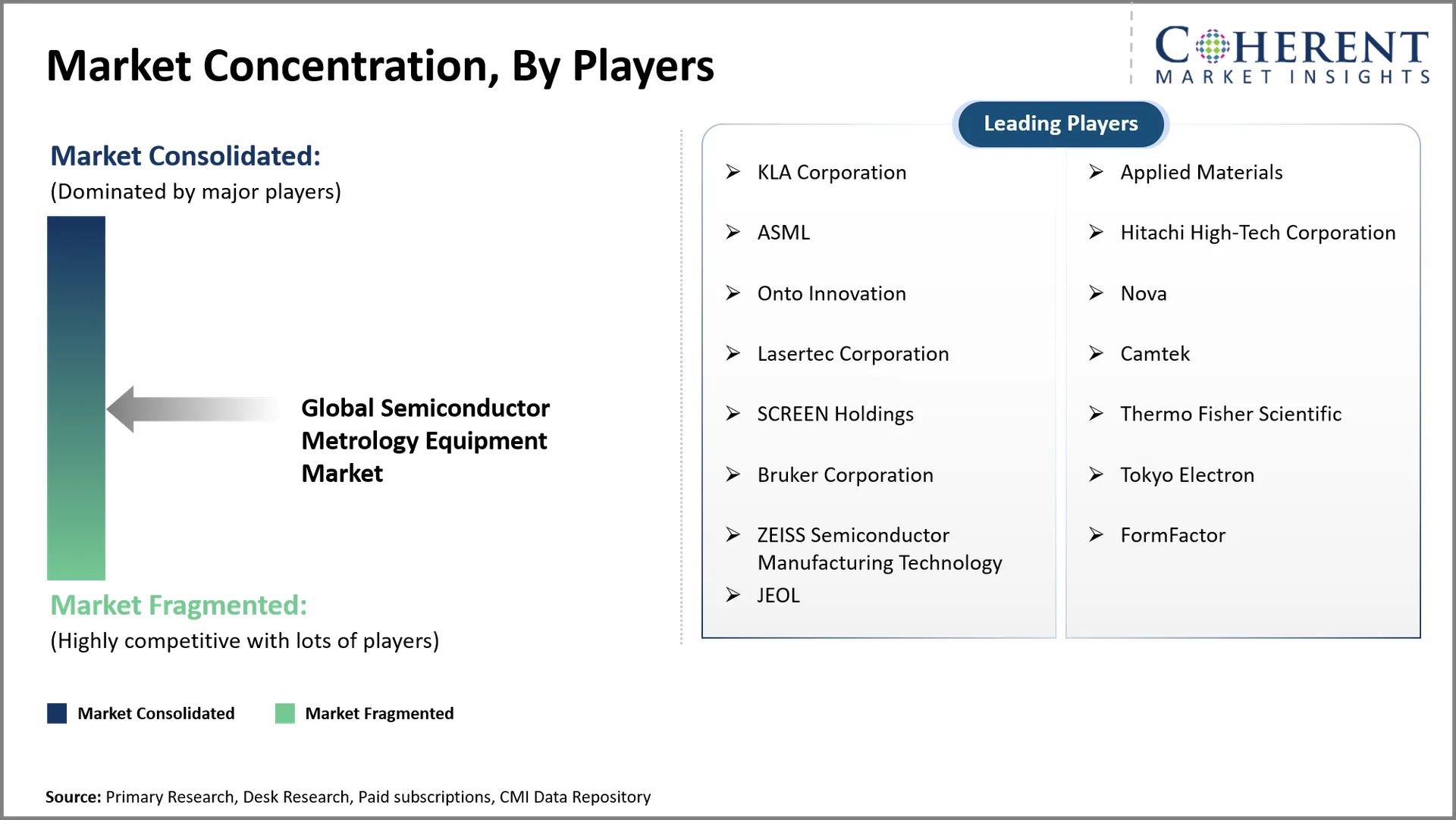
The competitive landscape is led by KLA Corporation, Applied Materials, ASML, Hitachi High-Tech Corporation, and Onto Innovation. KLA Corporation is expanding beyond wafer inspection into advanced packaging, substrates, software, and process-control analytics. Its 2026 portfolio covers inspection, metrology, defect review, and data analytics across logic, DRAM, 3D NAND, and packaging. Applied Materials is targeting artificial intelligence chips through e-beam metrology, defect review, DRAM, and advanced packaging. Its 2026 VeritySEM 7AP addresses critical-dimension measurement on warped and heterogeneous HBM substrates. Applied Materials also uses artificial intelligence across e-beam metrology and inspection workflows. KLA is strengthening packaging inspection through AI-based defect classification and substrate metrology.
Top Manufacturers and Notable Products
Manufacturer | Notable Product | Key features |
KLA Corporation | Archer Series | Optical overlay metrology, wafer alignment measurement, advanced process control, high-volume manufacturing support |
Applied Materials, Inc. | VeritySEM 7AP | Electron-beam critical dimension metrology, sub-10-nanometer sensitivity, support for warped substrates, high-bandwidth memory and chiplet applications |
ASML | YieldStar 1390 | High-throughput optical metrology, post-etch overlay measurement, advanced pattern control, mass-production process monitoring |
Hitachi High-Tech Corporation | GT2000 | High-precision electron-beam metrology, critical dimension measurement, High-NA extreme ultraviolet support, advanced-node process monitoring |
Onto Innovation Inc. | Dragonfly G5 | Advanced optical inspection, wafer-level process monitoring, defect detection, high-throughput inspection, advanced packaging applications |
Market Report Scope
Global Semiconductor Metrology Equipment Market Report Coverage | |||
Report Coverage | Details | ||
Base Year | 2025 | Market Size in 2026: | USD 16.00 Bn |
Historical Data For: | 2020 To 2024 | Forecast Period: | 2026 To 2033 |
Forecast Period 2026 To 2033 CAGR: | 9.60% | 2033 Value Projection: | USD 27.00 Bn |
Geographies covered: |
| ||
Segments covered: |
| ||
Companies covered: | KLA Corporation, Applied Materials, ASML, Hitachi High-Tech Corporation, Onto Innovation, Nova, Lasertec Corporation, Camtek, SCREEN Holdings, Thermo Fisher Scientific, Bruker Corporation, Tokyo Electron, ZEISS Semiconductor Manufacturing Technology, FormFactor, JEOL | ||
Growth Drivers: |
| ||
Restraints & Challenges: |
| ||
Analyst Opinion (Expert Opinion)
- The future of semiconductor metrology will shift toward integrated measurement ecosystems rather than standalone inspection tools. Advanced logic, HBM, chiplets, and three-dimensional packaging will require measurement across increasingly different surfaces and structures. E-beam systems will gain importance where optical resolution becomes insufficient. Applied Materials has already introduced e-beam systems specifically for advanced packaging applications. Artificial intelligence will become increasingly important for converting inspection data into immediate process decisions.
- The largest opportunity should emerge in advanced packaging, HBM, and gate-all-around transistor manufacturing. Advanced packaging deserves particular attention because stacked dies create new dimensional, alignment, and defect-control requirements. Applied Materials has developed VeritySEM 7AP for HBM and chiplet structures with sub-10-nanometer sensitivity. Taiwan, South Korea, and the U.S. should remain priority countries because they host intensive advanced logic and memory manufacturing. The strongest equipment opportunities should therefore concentrate on e-beam metrology, hybrid metrology, defect classification, and packaging inspection.
- Market players should build systems that combine measurement, defect review, classification, and process analytics. KLA demonstrates this direction by integrating inspection, metrology, software, and advanced packaging solutions. Suppliers should also develop application-specific platforms for HBM, chiplets, and gate-all-around structures. Partnerships with leading foundries and memory manufacturers can accelerate equipment qualification. Companies should prioritize measurement speed without sacrificing nanoscale sensitivity. Artificial intelligence should also become embedded within equipment workflows rather than remaining a separate software layer.
Speak to the analyst
Want personalized insights?
Take the findings above to one of our principal consultants, or have the report rebuilt around the segments, geographies and competitors you actually track.
Market Segmentation
- Type Insights (Revenue, USD Billion, 2021 - 2033)
- Optical Systems
- Beam Systems
- Dimension Insights (Revenue, USD Billion, 2021 - 2033)
- 2D Metrology and Inspection
- 3D Metrology and Inspection
- Hybrid 2D and 3D Systems
- Technology Type Insights (Revenue, USD Billion, 2021 - 2033)
- Wafer Inspection Systems
- Thin Film Metrology
- Mask Inspection Systems
- Package Inspection
- Others
- Process Node Insights (Revenue, USD Billion, 2021 - 2033)
- 7 Nanometers and Below
- 8 To 14 Nanometers
- 15 To 28 Nanometers
- Above 28 Nanometers
- Fab Type Insights (Revenue, USD Billion, 2021 - 2033)
- Foundries
- Integrated Device Manufacturers
- Memory Manufacturers
- Outsourced Semiconductor Assembly and Test Companies
- Regional Insights (Revenue, USD Billion, 2021 - 2033)
- North America
- U.S.
- Canada
- Latin America
- Brazil
- Argentina
- Mexico
- Rest of Latin America
- Europe
- Germany
- U.K.
- Spain
- France
- Italy
- Russia
- Rest of Europe
- Asia Pacific
- China
- India
- Japan
- Australia
- South Korea
- ASEAN
- Rest of Asia Pacific
- Middle East
- GCC Countries
- Israel
- Rest of Middle East
- Africa
- South Africa
- North Africa
- Central Africa
- North America
Sources
Primary Research Interviews
- Semiconductor Metrology Equipment Manufacturers
- Semiconductor Fabrication & Foundry Specialists
- Semiconductor Process Engineers & R&D Experts
- Supply Chain & Procurement Managers in Semiconductor Industry
Magazines
- Semiconductor Digest
- Solid State Technology
- IEEE Spectrum
Journals
- Journal of Vacuum Science & Technology
- Journal of Micro/Nanolithography, MEMS, and MOEMS
- Microelectronic Engineering (Elsevier)
Associations
- SEMI (Semiconductor Equipment and Materials International)
- Semiconductor Industry Association (SIA)
- International Society for Optics and Photonics (SPIE)
- European Semiconductor Industry Association (ESIA)
Public Domain Sources
- U.S. Geological Survey (USGS) – Semiconductor Minerals Data
- International Trade Administration (ITA) – Semiconductor Industry Reports
- World Semiconductor Trade Statistics (WSTS)
- U.S. International Trade Commission (USITC) Reports
Proprietary Elements
- CMI Data Analytics Tool
- Proprietary CMI Existing Repository of information for last 10 years
Get access to 250+ pages report
Every segment, forecast, competitor profile and data table behind the analysis above — available for instant download.
- ESOMAR Member
- ISO 9001:2015 Certified
- D-U-N-S Registered
- GDPR & CCPA Compliant
Frequently Asked Questions
The global semiconductor metrology equipment market is expected to stand at USD 16.00 Bn in 2026 and is expected to reach USD 27.00 Bn by 2033.
The CAGR of the global semiconductor metrology equipment market is projected to be 9.6% from 2026 to 2033.
Increasing semiconductor process complexity and Rising adoption of sub 7 nanometer nodes are the major factors driving the growth of the global semiconductor metrology equipment market.
High equipment acquisition costs and Complex equipment integration requirements are the major factors hampering the growth of the global semiconductor metrology equipment market.
In terms of type, optical systems segment is estimated to dominate the market revenue share in 2026.
Semiconductor metrology equipment measures critical dimensions, overlay, thickness, defects, and other parameters during semiconductor manufacturing.
Electron-beam metrology provides high-resolution measurements for extremely small semiconductor structures.