

Global Wafer Handling Robots Market Size and Forecast – 2026 To 2033
The global wafer handling robots market is expected to grow from USD 1.80 Bn in 2026 to USD 3.45 Bn by 2033, registering a compound annual growth rate (CAGR) of 6.2% from 2026 to 2033. The global wafer handling robots market is driven by growing demand for contamination-free wafer transportation industries. On June 17, 2025, KUKA introduced its KMR iisy CR cleanroom mobile manipulator for semiconductor applications. Consisting of a mobile platform and the six-axis LBR iisy CR robot, the KMR iisy CR is an optimal mobile manipulator for work in cleanrooms, owing to its low-particle and low-emission properties and Electrostatic Discharge (ESD) certification.
Key Takeaways of the Global Wafer Handling Robots Market
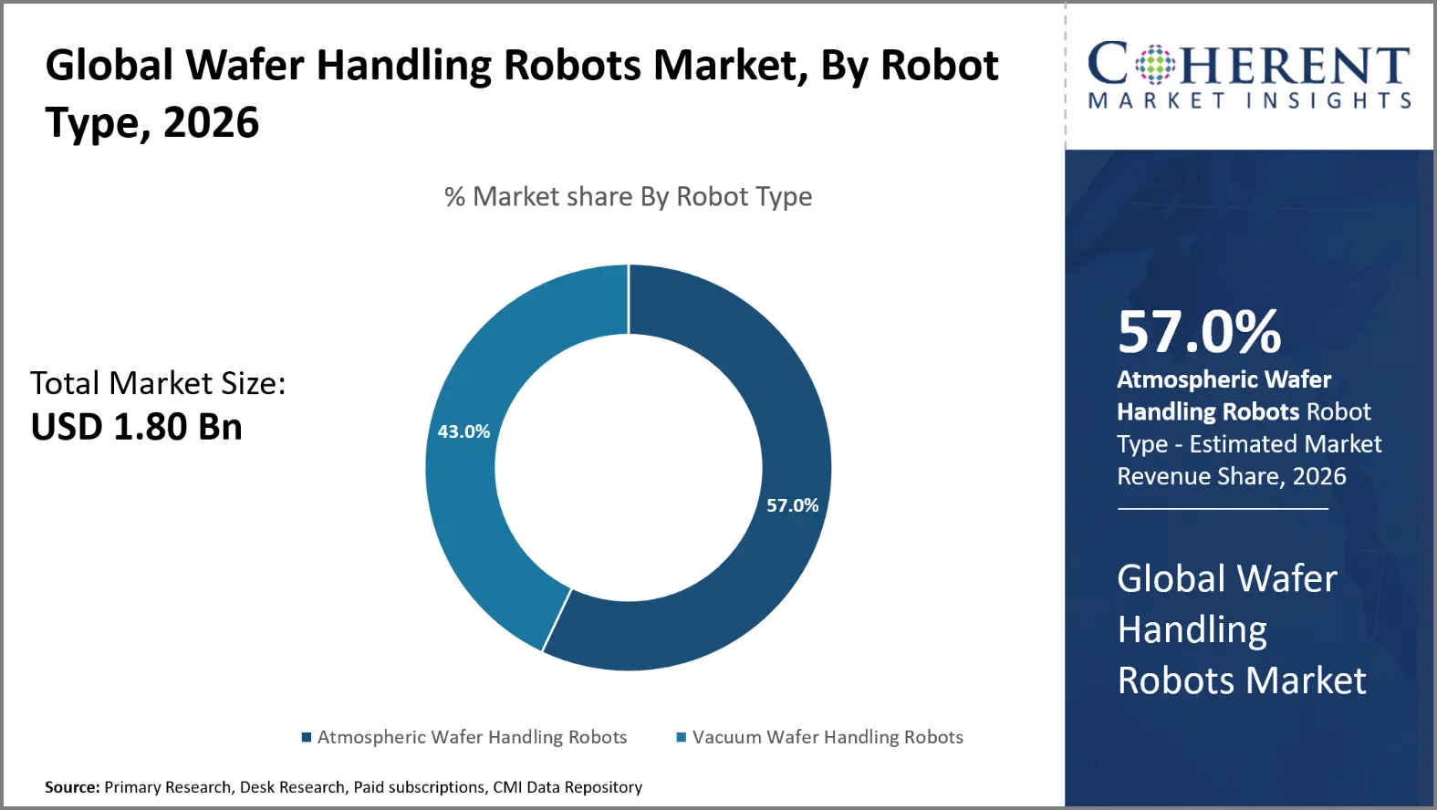
- The Atmospheric Wafer Handling Robots segment is expected to account for 57.0% of the global wafer handling robots market share in 2026. Expansion of advanced semiconductor packaging is driving the growth of the segment. On October 6, 2025, Amkor Technology broke ground on its advanced packaging and test campus in Arizona, U.S. The company expanded the planned investment to USD 7 billion across two phases.
- The Single-Arm Robots segment is estimated to capture 61.0% of the market share in 2026. Increasing production of artificial intelligence chips is majorly driving the growth of the segment. On June 12, 2025, Micron Technology announced approximately USD 200 billion for U.S. semiconductor manufacturing and research. The plan includes additional leading-edge memory fabs and domestic high-bandwidth memory packaging.
- The 300-millimeter Wafers segment is estimated to capture 78.0% of the market share in 2026. Growing adoption of 300-millimeter wafers is majorly driving the growth of the segment. On December 17, 2025, Texas Instruments Incorporated started production at its new 300-millimeter SM1 fab in Sherman, Texas, U.S. The facility can ultimately produce tens of millions of chips daily. The Sherman site includes plans for four connected 300-millimeter fabs.
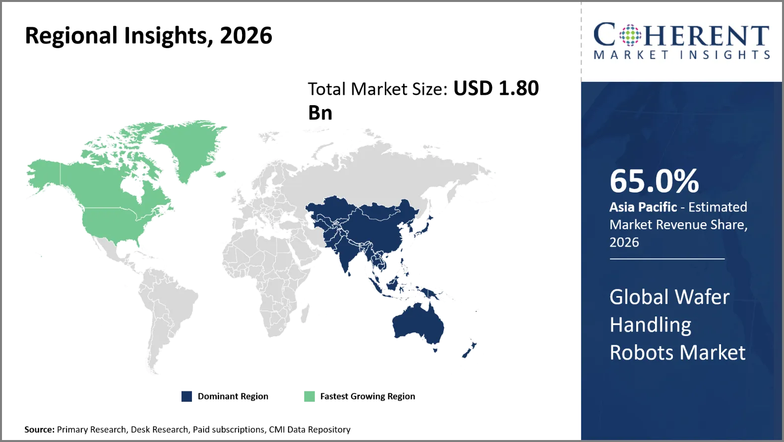
- Asia Pacific is expected to dominate the wafer handling robots market in 2026 with a market share of 65.0%. Increasing demand for vacuum transfer robots in Asia Pacific is driving the growth of the regional market. In December 2025, JEL Corporation exhibited its DTVFR ultra-high-vacuum transfer robot. The demonstration occurred at SEMICON Japan 2025. JEL positioned the robot for next-generation semiconductor manufacturing. The company highlighted high vacuum resistance and low leak-rate performance.
- North America is expected to account for 21.0% share in 2026 and is projected to record the fastest growth over the forecast period. Expansion of dual-arm robotic systems in North America is driving the growth of the regional market. In December 2025, AAE North America announced major capability expansion following its earlier Solara Automation acquisition. The company planned a state-of-the-art cleanroom and expansion toward a 100,000-square-foot facility.
Segmental Insights
Why Does Atmospheric Wafer Handling Robots Dominate the Global Wafer Handling Robots Market?
The atmospheric wafer handling robots segment is expected to account for 57.0% of the global wafer handling robots market share in 2026. Atmospheric wafer handling robots dominate because most semiconductor processes operate under controlled atmospheric conditions. The robots continuously transport wafers between load ports, aligners, process chambers and inspection tools. Their architectures facilitate high-throughput semiconductor production and relatively uncomplicated equipment integration. Atmospheric robots also offer automated material handling during several industrial phases. They can accommodate different wafer-handling sequences without requiring vacuum-compatible infrastructure. Their maintenance requirements are generally simpler than vacuum-based robotic systems. For instance, in 2025, JEL Corporation promoted its GTCR5280 atmospheric robot for 300-millimeter wafers. The five-axis robot operates directly within cleanroom atmospheric environments. Its twin end-effector provides functions similar to a twin-arm robot. The design can access three FOUPs without requiring a track. JEL also highlights reduced wafer swap time and automatic origin positioning.
- Current Industry Events of 2026
- Market Size Estimation
- Regional Breakdown
- Competitive Landscape
- Customer Intelligence
- Segmental Analysis
- Pricing Analysis
- Key Market Drivers, Challenges & Future Trends
- Customized Insights Section
Why is Single-Arm Robots the Most Preferred Configuration Type?
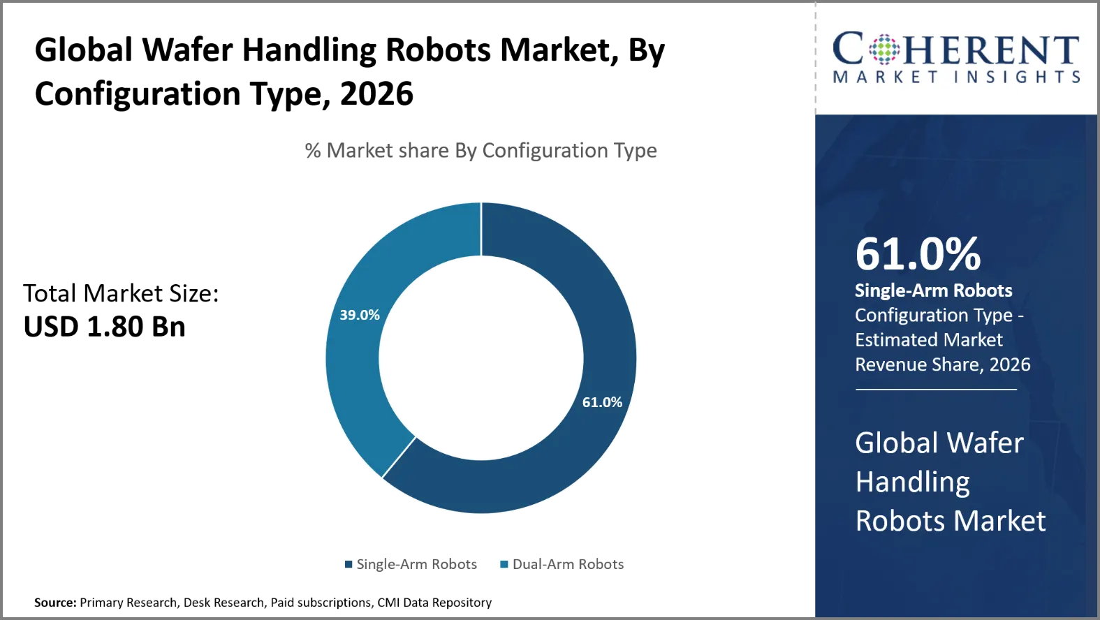
The single-arm robots segment is expected to account for 61.0% of the global wafer handling robots market share in 2026. Single-arm robots are still the most common, for they provide a good compromise between accuracy, versatility, and equipment cost. The small architecture is applicable to semiconductor fabrication equipment with little space inside. Single-arm design is able to transfer individual wafers between processing positions with high accuracy. They also make it easier to integrate with existing semiconductor equipment topologies. Manufacturers can design these robots to meet varied wafer sizes and process needs. They have a simplified mechanical design which can minimize maintenance complexity and potential sites of failure. In 2025, DAIHEN Corporation launched the UT-VDX3000NS single-arm robot to its ACTRANS range. The system handles wafers up to 300 millimeters under ultra-high-vacuum conditions. Its direct-drive motor reduces vibration during arm movement. The robot achieves 0.02-millimeter repeatability in the company’s specified conditions.
300-millimeter Wafers Dominates the Global Wafer Handling Robots Market
The 300-millimeter wafers segment is expected to account for 78.0% of the global wafer handling robots market share in 2026. 300-millimeter wafers dominate because modern semiconductor fabs increasingly rely on this wafer diameter. Larger wafers provide greater die output from each processed substrate. Higher die productivity improves manufacturing efficiency for advanced semiconductor devices. This indicates that semiconductor fabrication facilities must have automated systems designed for 300-millimeter wafer handling. These robots need to be positioned accurately, with little vibration or particle creation. They also match with standardized front-opening unified pod material handling systems.
On September 28, 2026, VisionPower Semiconductor Manufacturing Company Pte. Ltd., the joint venture established by Vanguard International Semiconductor Corporation and NXP Semiconductors N.V., officially opened its first 12-inch (300mm) fab in Tampines, Singapore. Once it reaches full capacity in 2029, the fab is planned to manufacture around 44,000 12-inch wafers a month and provide about 1,600 jobs.
Current Events and their Impact
Current Events | Description and its Impact |
European Chips Act, Regulation (EU) 2023/1781 |
|
U.S. Semiconductor Manufacturing Equipment Export Controls |
|
Wafer Handling Robots Market Dynamics
Market Drivers
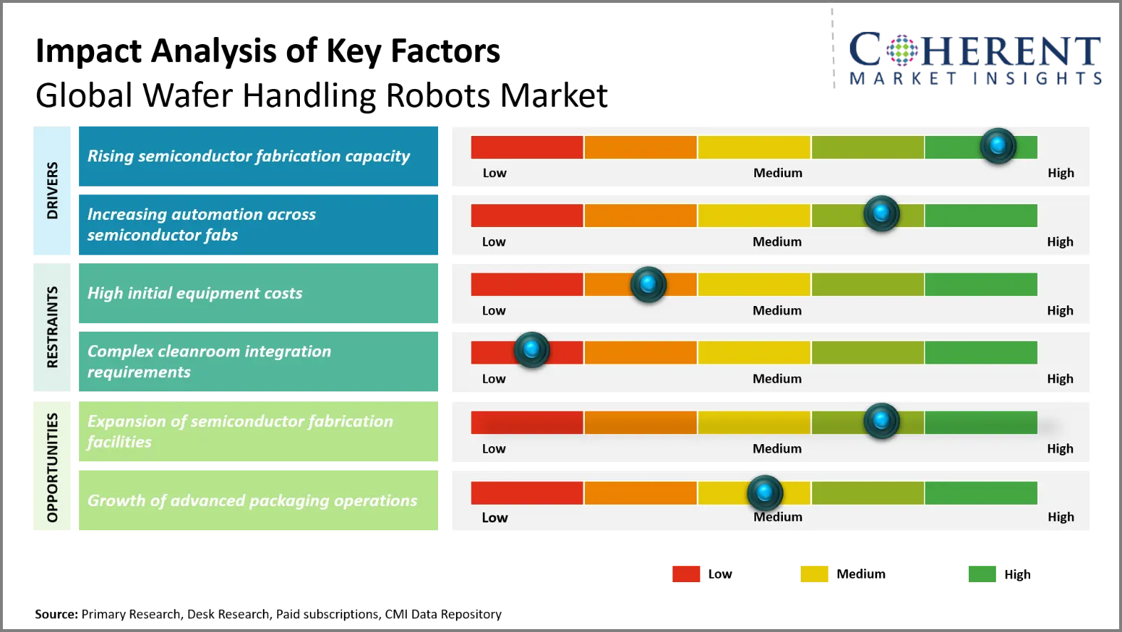
- Rising semiconductor fabrication capacity: Demand for wafer handling robots is growing in new and enlarged fabs as semiconductor production capacity increases. Governments are providing incentives and strategic industrial strategies to promote domestic semiconductor production. New fabrication facilities require automated wafer movement between process, inspection, and metrology equipment. Advanced logic, memory, power, and automotive semiconductor production are expanding equipment requirements. Larger fabrication projects also favor standardized robotic platforms supporting high-volume manufacturing. This capacity expansion creates sustained demand for atmospheric and vacuum wafer handling robots.
- On August 7, 2026, SK hynix Inc. announced that it has decided to build new fabs in Yongin and Cheongju, South Korea, to respond to the continuously growing demand for memory in the AI era. This decision represents execution of the mid-to-long-term investment strategy announced by the company in June, 2026.
- Increasing automation across semiconductor fabs: Growing automation across semiconductor fabs is bolstering demand for reliable wafer handling robots. To enhance consistency, throughput and contamination control, manufacturers are decreasing manual material movement. Integration with factory automation systems also allows for coordinated material movement and production monitoring. Automation adoption is expanding as semiconductor processes become more complex and production volumes increase.
- On December 11, 2025, Siemens and GlobalFoundries (GF) entered a new strategic collaboration to leverage each company’s complementary AI-based capabilities to enhance performance of semiconductor manufacturing and advanced industries. In their latest memorandum of understanding, the companies focus on automation technologies for semiconductor fabrication (fab automation), electrification, digital solutions and software ranging from chip development to product lifecycle management.
Market Restraints
- High equipment integration costs: Wafer handling robots require specialized cleanroom integration, precision controls, and compatibility with semiconductor processing equipment. High installation, validation, and commissioning costs can discourage smaller fabs from adopting advanced robotic systems. Existing facilities may also require costly infrastructure modifications.
- Complex maintenance and contamination risks: Wafer handling robots function under rigorous cleanliness and precision standards. Expensive wafers are damaged by mechanical failures, particle production or placement problems. Robotic precision assumes trained experts, preventive maintenance and strict contamination control methods throughout the entire semiconductor manufacturing environment.
Emerging Trends
- AI-enabled predictive maintenance: Artificial intelligence is increasingly being used to help with predictive maintenance of wafer handling robots. Manufacturers examine data on motion, vibration and equipment performance to try to detect probable breakdowns. This method decreases unplanned downtime, enhances robot readiness, and contributes to more stable semiconductor manufacturing.
- Advanced dual-arm robotic architectures: Dual-arm wafer handling robots are receiving interest since they can improve the efficiency of material transfer. Their arms are synchronized and can hold numerous wafers in successive operations. This architecture meets increased throughput needs for advanced semiconductor fabrication settings.
- Greater 300-millimeter wafer automation: The rise of 300-millimeter semiconductor manufacturing is driving robots designed for larger wafer substrates. Manufacturers are designing systems with higher positioning precision, less vibration, and more contamination control. These features help sophisticated fabrication processes needing precise, repeatable wafer manipulation.
- Integration with intelligent factory automation: Wafer-handling robots are being incorporated into new-generation semiconductor factory automation platforms. Connected systems coordinate wafer mobility, equipment condition, production schedule and process details. This incorporation enhances traceability, equipment utilization, and production efficiency in the increasingly automated manufacturing operations.
Regional Insights
Why is Asia Pacific a Strong Market for Wafer Handling Robots?
Asia Pacific is expected to account for a market share of 65.0% in 2026. It remains the largest manufacturing base for wafer handling robots because semiconductor production is deeply concentrated there. China, Taiwan, South Korea, and Japan collectively represented 87% of global in-production wafer capacity in September 2025. The region is also seeing substantial new fab construction. Eighteen new fabs were scheduled globally for 2025, including projects across Japan, China, Taiwan, and Korea. High-volume 300-millimeter production strengthens demand for automated wafer transfer equipment. Artificial intelligence memory, advanced logic, automotive chips, and power semiconductors provide distinct automation requirements. Regional equipment suppliers also support localized installation, maintenance, and process-integration capabilities.
Why Does North America Wafer Handling Robots Market Exhibit High Growth?
North America is expected to register the fastest growth with a CAGR of 8.0% over the forecast period and is projected to account for 21.0% of the global wafer handling robots market in 2026. North America is expanding wafer handling robot demand through accelerated domestic semiconductor manufacturing investment. Four new semiconductor fabrication projects were expected to begin construction across the Americas during 2025. TSMC Arizona began 4-nanometer volume production during the fourth quarter of 2024. Its second facility is being prepared for 3-nanometer and more advanced technologies. New facilities require automated wafer transfer between fabrication, inspection, metrology, and packaging equipment. Advanced packaging expansion also increases demand for contamination-controlled robotic movement. Equipment localization is becoming increasingly important as North American manufacturers strengthen domestic semiconductor supply chains.
Global Wafer Handling Robots Market Outlook for Key Countries
Why is China Emerging as a Major Hub in the Wafer Handling Robots Market?
China is experiencing strong wafer handling robot demand because semiconductor manufacturers continue expanding domestic fabrication capacity. Chinese semiconductor capacity was projected to increase 14% during 2025, reaching almost one-third of global capacity. Semiconductor manufacturers including Semiconductor Manufacturing International Corporation, Hua Hong Semiconductor, Nexchip Semiconductor Corporation, and ChangXin Memory Technologies are expanding production. Export restrictions are also encouraging greater domestic development of semiconductor manufacturing equipment. This environment creates opportunities for Chinese robotic suppliers serving localized fabrication equipment ecosystems. Demand spans mature-node automotive chips, power devices, memory, and increasingly advanced logic production.
Is U.S. the Next Growth Engine for the Wafer Handling Robots Market?
The U.S. wafer handling robots market is benefiting from large-scale fabrication projects supported by domestic semiconductor policies. Samsung Electronics received up to USD 4.745 billion under the CHIPS and Science Act in December 2024. Samsung plans two leading-edge logic fabs and research facilities in Taylor, Texas. TSMC Arizona also started constructing its third facility during 2025. These projects require automated wafer movement across increasingly complex production environments. Intel, Micron Technology, and other manufacturers are similarly strengthening domestic capabilities. The resulting ecosystem is supporting demand for advanced robotic automation, integration, and service infrastructure.
Taiwan Wafer Handling Robots Market Analysis and Trends
Taiwan remains a critical wafer handling robot market because Taiwan Semiconductor Manufacturing Company operates an extensive domestic fabrication network. Its Taiwanese facilities include six 12-inch GIGAFAB fabs, four 8-inch fabs, and one 6-inch fab. Taiwan Semiconductor Manufacturing Company produced advanced technologies supporting high-performance computing and artificial intelligence applications. Its domestic manufacturing scale creates continuous requirements for automated wafer transfer and equipment integration. Taiwan was also expected to maintain the world's second-largest semiconductor fabrication capacity during 2025. The concentration of advanced manufacturing encourages adoption of high-precision robots supporting stringent throughput and contamination requirements.
Japan Wafer Handling Robots Market Analysis and Trends
Japan is expanding wafer handling robot demand through new advanced semiconductor projects and domestic technology development. Rapidus Corporation received approval for its fiscal 2025 plans supporting 2-nanometer semiconductor integration technologies. TSMC's Japan Advanced Semiconductor Manufacturing facility began volume production at its first facility during late 2024. Construction of a second facility began during 2025. Japan also had four semiconductor fab projects scheduled to begin construction during 2025. These projects create demand for cleanroom-compatible robots supporting advanced logic, automotive, industrial, and specialty semiconductor manufacturing.
South Korea Wafer Handling Robots Market Analysis and Trends
South Korea is a major wafer handling robot market because memory manufacturing requires continuous process scaling and automation upgrades. Nearly 80% of Korea's wafer capacity falls within process nodes between 6 and below 22 nanometers. Samsung Electronics and SK hynix drive substantial demand for advanced memory manufacturing equipment. High-bandwidth memory production is expanding alongside artificial intelligence server demand. Semiconductor manufacturers are increasing investment in dynamic random-access memory and high-bandwidth memory technologies. These production environments require highly repeatable wafer transfers across deposition, etching, inspection, and packaging stages. This specialization strengthens demand for precision robotic handling systems.
Global Wafer Handling Robots Market - Wafer Handling Robot Installations by Country (2025)
Country | Estimated Robot Installations |
China | 3,850 |
Taiwan | 2,950 |
South Korea | 2,450 |
Japan | 950 |
U.S. | 900 |
Singapore | 420 |
Germany | 260 |
Malaysia | 210 |
India | 120 |
France | 90 |
How is Expansion of Semiconductor Fabrication Facilities Creating New Growth Opportunities in the Wafer Handling Robots Market?
Expansion of semiconductor fabrication facilities is creating new opportunities by increasing the number of automated wafer-transfer points inside modern fabs. TSMC is building additional Arizona fabs supporting 2-nanometer and advanced technologies, requiring extensive cleanroom material automation. Rapidus is developing a 2-nanometer production facility in Japan, creating demand for precision wafer transport infrastructure. Samsung is expanding its Taylor, Texas manufacturing complex with leading-edge logic fabs. China is also adding fabrication capacity across mature and advanced process technologies. Each new fab requires robots for wafer movement between process chambers, load ports, inspection stations, and stockers. This expansion favors suppliers offering contamination control, high repeatability, and integration with factory automation systems.
On April 16, 2026, the Indian government notified a dedicated Special Economic Zone for Tata Semiconductor Manufacturing. The facility is planned across 66.166 hectares in Dholera, Gujarat. The project represents India's first semiconductor fabrication plant.
Market Players, Key Development, and Competitive Intelligence
Key Developments
- On December 10, 2025, RORZE announced it will exhibit a working model of the newly developed wrist technology, the Flap Wrist, as a new technology at SEMICON Japan 2025. This is a technology demonstration of a wrist mechanism in which the robot’s fingers move to adapt to various wafer shapes, accurately and securely hold them using vacuum suction, and transfer them.
- On September 1, 2025, Taiwan Hirata Corporation, a subsidiary of Hirata Corporation, announced it will be exhibiting at SEMICON Taiwan 2025. The exhibits consist of Hirata Corporation’s latest innovations, including a new type of load port and newly developed operational robots.
- On June 19, 2025, Yaskawa Electric Corporation announced that Yaskawa America Inc. plans to establish a new campus in Franklin, Wisconsin, with a USD 180 million investment over the next eight to ten years which will include relocating its headquarters and production functions in Illinois and Wisconsin.
Competitive Landscape
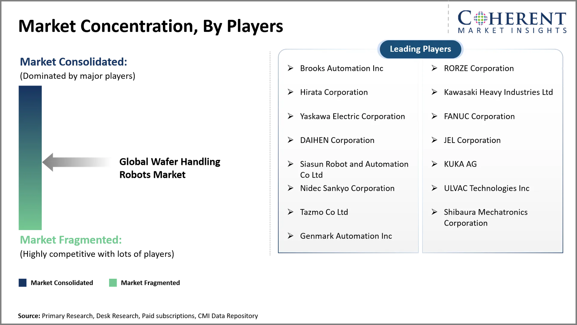
Leading players are differentiating through precision robotics, contamination control, advanced packaging, and application-specific automation. Brooks Automation focuses on vacuum robotics, atmospheric solutions, contamination control, and advanced packaging. Its installed base includes more than 70,000 wafer-handling robots. RORZE Corporation emphasizes low-particle, high-throughput semiconductor automation. Its portfolio spans atmospheric robots, vacuum robots, aligners, load ports, and equipment front-end modules. RORZE also introduced its Flap Wrist technology for secure handling of varied wafer shapes. Hirata Corporation focuses on integrated equipment front-end modules, load ports, aligners, and wafer robots. Its AR-Wn180CL platform combines single-arm and twin-arm configurations with vibration suppression.
Top Manufactures And Their Notable Products
Manufacturer | Notable Product | Key features |
Brooks Automation | MagnaTran LEAP Vacuum Robot | High-precision vacuum wafer transfer, direct-drive technology, configurable architectures, support for 300-millimeter wafers, long operating life |
RORZE Corporation | RORZE Vacuum Robot Series | High-speed wafer transfer, low-particle operation, precision positioning, atmospheric and vacuum configurations, advanced semiconductor equipment integration |
Hirata Corporation | AR-Wn Series | 300-millimeter and 450-millimeter wafer handling, direct-drive motors, vibration below 0.1G, high throughput, collision detection, easy maintenance |
DAIHEN Corporation | ACTRANS UT-VDX3000NS | Single-arm architecture, 300 millimeter wafer handling, direct-drive motor, ultra-high-vacuum operation, ISO Class 1 cleanliness, 0.02-millimeter repeatability |
JEL Corporation | GTCR5280 | Atmospheric 300-millimeter wafer handling, five-axis movement, compact configuration, multiple FOUP access, flexible end-effector options |
Market Report Scope
Global Wafer Handling Robots Market Report Coverage | |||
Report Coverage | Details | ||
Base Year | 2025 | Market Size in 2026: | USD 1.80 Bn |
Historical Data For: | 2020 To 2024 | Forecast Period: | 2026 To 2033 |
Forecast Period 2026 To 2033 CAGR: | 6.20% | 2033 Value Projection: | USD 3.45 Bn |
Geographies covered: |
| ||
Segments covered: |
| ||
Companies covered: | Brooks Automation Inc, RORZE Corporation, Hirata Corporation, Kawasaki Heavy Industries Ltd, Yaskawa Electric Corporation, FANUC Corporation, DAIHEN Corporation, JEL Corporation, Siasun Robot and Automation Co Ltd, KUKA AG, Nidec Sankyo Corporation, ULVAC Technologies Inc, Tazmo Co Ltd, Shibaura Mechatronics Corporation, Genmark Automation Inc | ||
Growth Drivers: |
| ||
Restraints & Challenges: |
| ||
Analyst Opinion (Expert Opinion)
- The industry is moving toward tightly integrated robotic ecosystems rather than standalone wafer transfer arms. Future systems will combine robotics, contamination control, diagnostics, and factory-level communication. Vacuum automation should remain strategically important for advanced logic and memory processes. Advanced packaging will create another growth avenue as substrates become larger and process flows become more complex. Robots capable of maintaining precision under thermal, vibration, and cleanliness constraints will gain stronger customer preference.
- The strongest opportunities should emerge in vacuum robots, advanced packaging automation, and 300-millimeter handling systems. Taiwan and South Korea offer attractive opportunities because advanced logic and memory manufacturing require highly controlled wafer movement. The U.S. also offers major opportunity as new fabrication capacity requires localized automation. Suppliers with excellent domestic engineering, component availability and compliance capabilities have prospects in China.
- Players should differentiate through application-specific engineering rather than solely compete on robot hardware specifications. Brooks showcases the power of the combination of robots with contamination control, diagnostics and lifecycle servicing. RORZE also benefits from large semiconductor automation portfolios and localized overseas operations. The key is speedy qualification, predictive diagnostics, modular designs, regional service networks. These features can help reduce client integration risks, while increasing equipment uptime and long-term ownership economics.
Speak to the analyst
Want personalized insights?
Take the findings above to one of our principal consultants, or have the report rebuilt around the segments, geographies and competitors you actually track.
Market Segmentation
- Robot Type Insights (Revenue, USD Billion, 2021 - 2033)
- Atmospheric Wafer Handling Robots
- Vacuum Wafer Handling Robots
- Configuration Type Insights (Revenue, USD Billion, 2021 - 2033)
- Single-Arm Robots
- Dual-Arm Robots
- Wafer Size Insights (Revenue, USD Billion, 2021 - 2033)
- 300-Millimeter Wafers
- 200-Millimeter Wafers
- Others
- Application Insights (Revenue, USD Billion, 2021 - 2033)
- Front-End Processing
- Back-End assembly and Packaging
- Inspection and Metrology
- End User Insights (Revenue, USD Billion, 2021 - 2033)
- Integrated Device Manufacturers
- Semiconductor Foundries
- Outsourced Semiconductor Assembly and Test Providers
- Regional Insights (Revenue, USD Billion, 2021 - 2033)
- North America
- U.S.
- Canada
- Latin America
- Brazil
- Argentina
- Mexico
- Rest of Latin America
- Europe
- Germany
- U.K.
- Spain
- France
- Italy
- Russia
- Rest of Europe
- Asia Pacific
- China
- India
- Japan
- Australia
- South Korea
- ASEAN
- Rest of Asia Pacific
- Middle East
- GCC Countries
- Israel
- Rest of Middle East
- Africa
- South Africa
- North Africa
- Central Africa
- North America
Sources
Primary Research Interviews
- Wafer Handling Robot Manufacturers & OEMs
- Semiconductor Fabrication Facility (Fab) Managers
- Automation & Robotics System Integrators
- Semiconductor Equipment Distributors & Suppliers
Magazines
- Semiconductor Digest
- Solid State Technology
- Robotics Business Review
- IEEE Spectrum Magazine
Journals
- Journal of Vacuum Science & Technology
- IEEE Transactions on Semiconductor Manufacturing
- International Journal of Advanced Robotic Systems
Associations
- SEMI (Semiconductor Equipment and Materials International)
- International Federation of Robotics (IFR)
- Robotic Industries Association (RIA) / A3 Automate
- Semiconductor Industry Association (SIA)
Public Domain Sources
- U.S. Securities and Exchange Commission (SEC) Filings
- World Semiconductor Trade Statistics (WSTS)
- United States International Trade Commission (USITC) Reports
- European Commission – Digital Industry Reports
Proprietary Elements
- CMI Data Analytics Tool
- Proprietary CMI Existing Repository of Information for the Last 10 Years
Get access to 250+ pages report
Every segment, forecast, competitor profile and data table behind the analysis above — available for instant download.
- ESOMAR Member
- ISO 9001:2015 Certified
- D-U-N-S Registered
- GDPR & CCPA Compliant
Frequently Asked Questions
The global wafer handling robots market is expected to stand at USD 1.80 Bn in 2026 and is expected to reach USD 3.45 Bn by 2033.
The CAGR of the global wafer handling robots market is projected to be 6.2% from 2026 to 2033.
Rising semiconductor fabrication capacity and Increasing automation across semiconductor fabs are the major factors driving the growth of the global wafer handling robots market.
High initial equipment costs and Complex cleanroom integration requirements are the major factors hampering the growth of the global wafer handling robots market.
In terms of robot type, atmospheric wafer handling robots segment is estimated to dominate the market revenue share in 2026.
Wafer handling robots automatically transport semiconductor wafers between manufacturing, inspection, metrology, and storage equipment.
A vacuum robot transfers wafers between process chambers operating under vacuum conditions.