

Global Advanced IC Substrate Market Size and Forecast – 2026 To 2033
The global advanced IC substrate market is expected to grow from USD 18.00 Bn in 2026 to USD 33.00 Bn by 2033, registering a compound annual growth rate (CAGR) of 8% from 2026 to 2033. The global advanced IC substrate market is driven by rising high-bandwidth memory integration in data center processors. On February 12, 2026, Samsung Electronics announced that it has begun mass production of its industry-leading HBM4 and has shipped commercial products to customers. This achievement marks a first in the industry, securing an early leadership position in the HBM4 market.
Key Takeaways of the Global Advanced IC Substrate Market
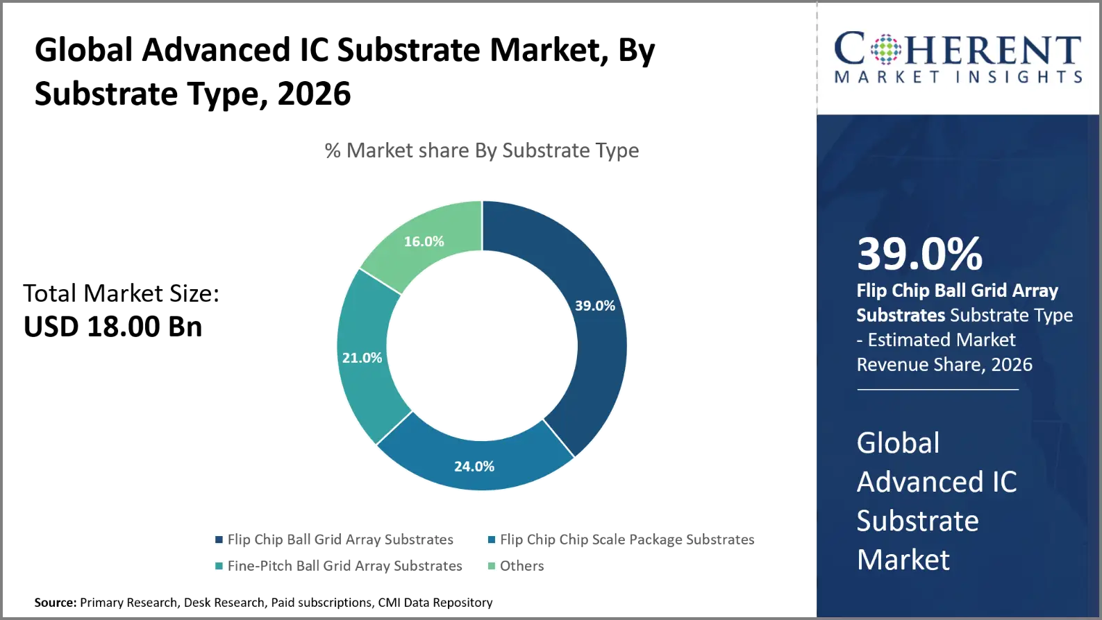
- The Flip Chip Ball Grid Array Substrates segment is expected to account for 39.0% of the global advanced IC substrate market share in 2026. Expansion of automotive electronics and advanced driver assistance systems is driving the growth of the segment. On June 9, 2026, NXP Semiconductors announced the SAF8444 automotive radar system-on-chip for advanced driver assistance systems.
- The High-Density Interconnect Substrates segment is estimated to capture 37.0% of the market share in 2026. Increasing demand for compact and high-density electronic packages is majorly driving the growth of the segment. On September 10, 2026, Samsung Electro-Mechanics presented next-generation semiconductor package substrates at the Korea Printed Circuit Association exhibition.
- The Consumer Electronics segment is estimated to capture 41.0% of the market share in 2026. Growing demand for advanced substrates supporting chiplet integration is majorly driving the growth of the segment. On May 28, 2025, Advanced Semiconductor Engineering revealed its FOCoS-Bridge packaging technology with through-silicon vias. The design shortens interconnection paths and improves input-output density and thermal dissipation for artificial intelligence and high-performance computing applications.
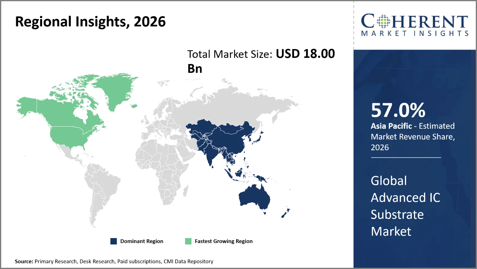
- Asia Pacific is expected to dominate the advanced IC substrate market in 2026 with a market share of 57.0%. Expansion of domestic semiconductor packaging capacity in Asia Pacific is driving the growth of the regional market. On October 3, 2025, Advanced Semiconductor Engineering held a groundbreaking ceremony for its K18B factory in Kaohsiung, Taiwan. The facility is scheduled for completion in the first quarter of 2028.
- North America is expected to account for 22.0% share in 2026 and is projected to record the fastest growth over the forecast period. Development of high-density substrates for automotive and networking applications in North America is driving the growth of the regional market. On February 25, 2026, AGY and JPS Composite Materials announced a partnership to produce North America’s first low-coefficient-of-thermal-expansion glass fiber fabric specifically designed for advanced integrated circuit substrates.
Segmental Insights
Why Does Flip Chip Ball Grid Array Substrates Dominate the Global Advanced IC Substrate Market?
The flip chip ball grid array substrates segment is expected to account for 39.0% of the global advanced IC substrate market share in 2026. Flip chip ball grid array substrates are commonly utilized because high input-output density, quicker signal transfer and efficient electrical connection can be supported. In modern semiconductor packages, interconnects are short, which reduces parasitic effects and improves performance. Such substrates also provide for efficient heat dissipation and small packaging designs. Increasing demand for graphics processing units, artificial intelligence accelerators, networking processors and high-performance computing systems boosts their importance. They are compatible with sophisticated packaging technologies making them ideal for increasingly complicated integrated circuit. Their continual progress in substrate manufacturing also promotes their use in applications of computing, telecommunications, and consumer electronics.
On October 21, 2026, Samsung Electro-Mechanics announced that it will join with NVIDIA to boost the global AI semiconductor supply chain and expedite the growth of next-generation AI infrastructure. Under the deal, the two businesses will jointly invest to expand dedicated manufacturing facilities for ABF package substrates used in AI semiconductors.
- Current Industry Events of 2026
- Market Size Estimation
- Regional Breakdown
- Competitive Landscape
- Customer Intelligence
- Segmental Analysis
- Pricing Analysis
- Key Market Drivers, Challenges & Future Trends
- Customized Insights Section
Why is High-Density Interconnect Substrates the Most Crucial Technology Type?
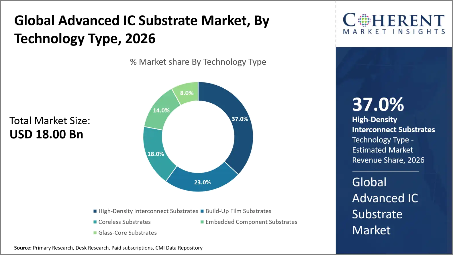
The high-density interconnect substrates segment is expected to account for 37.0% of the global advanced IC substrate market share in 2026. High density interconnect substrates are important because new integrated circuits require more connections in smaller and smaller package dimensions. Their thin conductive lines and tightly spaced interconnections allow for greater wiring density, and better signal routing. This enables manufacturers to handle complicated chip layouts while also managing package size. High-Density Interconnect technology also enables improved packaging designs for mobile CPUs, networking devices and high-performance computer systems. The increasing use of chiplets and high bandwidth memory introduces extra needs for accurate interconnects. Hence, manufacturers are upgrading circuit patterning, dielectric materials and manufacturing accuracy to satisfy the increasing performance requirements.
On September 9, 2025, Nitto Denko stated that it had signed a joint development agreement with IBM on research on new packaging materials. The collaboration will evaluate polymer materials for next-generation redistribution-layer technologies.
Consumer Electronics Dominates the Global Advanced IC Substrate Market
The consumer electronics segment is expected to account for 41.0% of the global advanced IC substrate market share in 2026. Consumer electronics represents a major application segment because smartphones, tablets, laptops, gaming devices, and wearable products require increasingly sophisticated semiconductor components. Advanced IC substrates provide dense packing, dependable electrical interconnection and efficient performance in these space-constrained systems. Increased demand for smartphones with artificial intelligence capabilities, high-resolution displays and power-efficient processors adds to packaging complexity. Manufacturers also demand substrates that offer more functionality without considerably increasing the size of the gadget. Product improvements, frequent upgrades and increasing integration of wireless connectivity, image processing and power management are driving demand. Large-scale consumer electronics production consequently supports sustained substrate consumption across established and emerging manufacturing markets.
On October 12, 2025, Murata Manufacturing Co., Ltd announced the World’s First LCP (liquid crystal polymer) flexible substrate with an Inner Cavity structure, ULTICIRC. Murata's original design incorporates an Inner Cavity in the substrate to realize a dielectric constant (Dk) of less than 2.0, so greatly cutting down the transmission loss.
Current Events and their Impact
Current Events | Description and its Impact |
U.S. - CHIPS and Science Act (Public Law 117-167) |
|
European Chips Act Regulation (EU) 2023/1781 |
|
Advanced IC Substrate Market Dynamics
Market Drivers
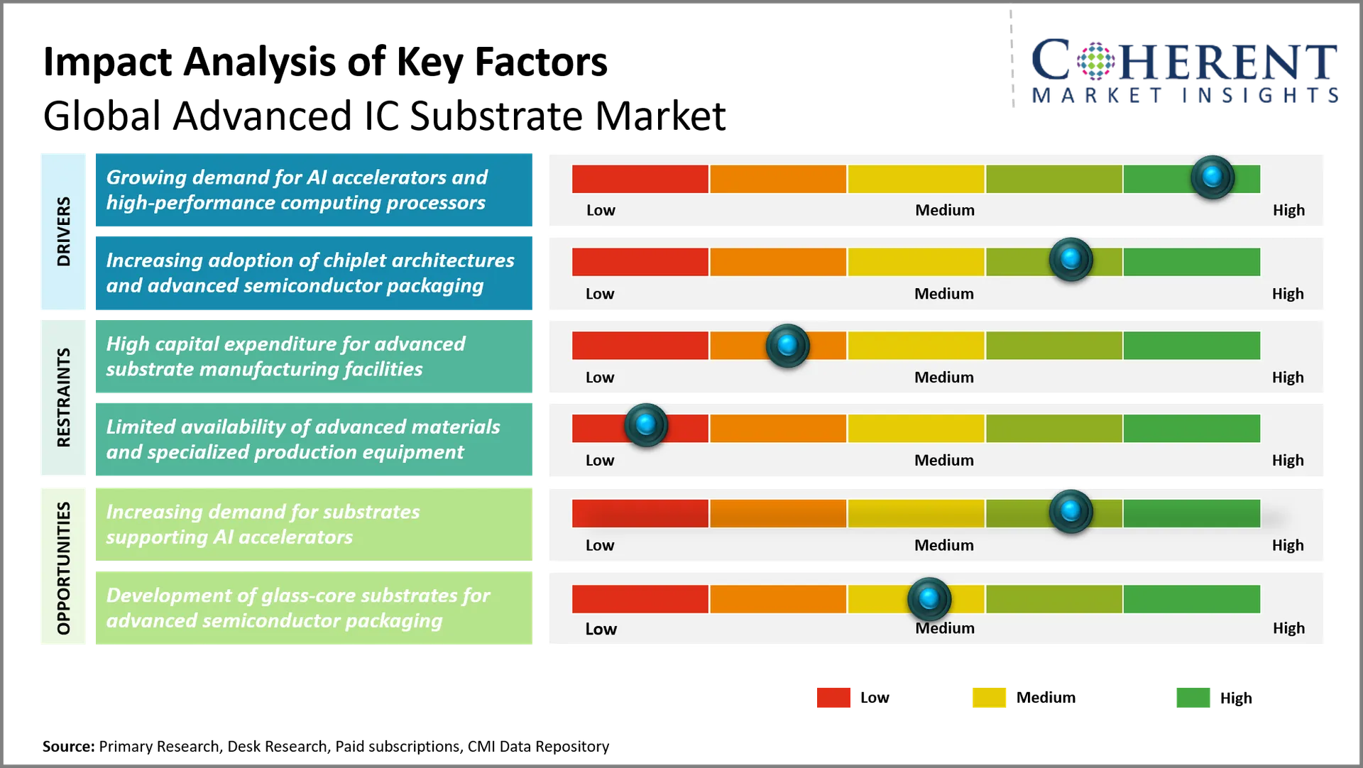
Growing demand for AI accelerators and high-performance computing processors
Increasing demand for artificial intelligence accelerators and high-performance computing processors is driving the advanced IC substrate market. Generative artificial intelligence, huge language models and other complicated computational workloads need processors with higher bandwidth and processing efficiency. These processors rely on improved substrates for high density electrical connectors, reliable signal transmission and efficient thermal management. The inclusion of high-bandwidth memory adds additional complexity and manufacturing constraints to the substrate. Hyperscale data centers and cloud computing providers are building out infrastructure to serve heavy AI workloads. This is pushing semiconductor makers to invest in new packaging technologies and high-performance substrates to enhance processor connectivity, power supply and overall computing performance.
On June 24, 2026, OpenAI and Broadcom launched Jalapeño, OpenAI’s first Intelligence Processor, an accelerator built around OpenAI’s vision for the future of LLM inference, and the first AI accelerator in a multi-generation compute platform.
Increasing adoption of chiplet architectures and advanced semiconductor packaging
Increasing adoption of chiplet architectures and advanced semiconductor packaging is driving demand for advanced IC substrates. Chiplet designs combine numerous tiny semiconductor dies within a single package for improved functionality, manufacturing flexibility and design efficiency. Such setups demand substrates with delicate circuit patterns, high connector density, and accurate electrical routing. Packaging is becoming more sophisticated with advanced technologies such as two-point-five-dimensional packaging and three-dimensional integration. Advanced substrates enable the interconnect of processing units, memory components and specialized accelerators in small packages. These architectures are being adopted by semiconductor companies to break beyond traditional chip-design limits and ramp up performance. This transition provides opportunity for substrate makers to develop finer geometries and multilayer connectivity methods.
On May 21, 2026, AMD announced an investment of more than USD 10 billion in the Taiwan ecosystem to strengthen key alliances and ramp advanced packaging manufacturing for next-generation AI infrastructure. AMD is working with critical partners in Taiwan and throughout the world to develop advanced silicon, packaging and manufacturing technologies that improve the performance, efficiency and speed of deployment of artificial intelligence (AI) systems.
Emerging Trends
- Adoption of glass-core substrate technology: Producers are investigating the use of glass-core substrates to improve dimensional stability, reduce warpage and allow for finer interconnections. These qualities are beneficial for big semiconductor packages for artificial intelligence accelerators, high-performance computer processors and enhanced memory integration.
- Expansion of advanced packaging and chiplet integration: Semiconductor makers are embracing chiplet architectures to combine specialized dies in small packages. This generates a need for substrates capable of hosting dense interconnections and accurate signal routing and dependable communication between processors, memory elements and dedicated computing units.
- Development of substrates for artificial intelligence processors: The growing artificial intelligence workloads are pushing manufacturers to build substrates with better electrical performance and power delivery. Such substrates allow for high bandwidth memory integration, greater package sizes and complicated interconnections needed for new accelerators and data center CPUs.
- Investment in ultra-fine circuit manufacturing: Substrate makers are working on lithography, laser processing and build-up technologies to generate finer circuit layouts. These characteristics offer better interconnection density in smaller form factors, enabling future generation semiconductor packages for networking equipment, mobile processors and high-performance computer applications.
Regional Insights
Why is Asia Pacific a Strong Market for Advanced IC Substrate?
Asia Pacific is expected to account for a market share of 57.0% in 2026. Asia Pacific draws advantage from the concentration of advanced substrate producers, semiconductor foundries, packaging facilities and specialist material suppliers. Taiwan adds significant flip-chip substrate capacity using Unimicron Technology, Nan Ya Printed Circuit Board and Kinsus Interconnect Technology. Ibiden of Japan and Shinko Electric Industries provide high-performance package substrates. South Korea offers experience in substrate production as well as memory and semiconductor packaging. China is supporting regional production through homegrown vendors like Shennan Circuits. Japan’s Ibiden said it would invest about 500 billion yen in electronics over fiscal 2026-2028, primarily in high-performance substrates for servers that run artificial intelligence.
Why Does North America Advanced IC Substrate Market Exhibit High Growth?
North America is expected to register the fastest growth with a CAGR of 8.3% over the forecast period. It is projected to account for 22.0% of the global advanced IC substrate market in 2026. The region is strengthening its advanced IC substrate ecosystem through semiconductor supply-chain diversification and investment in domestic packaging capabilities. Artificial intelligence infrastructure, cloud computing, aircraft electronics and high-performance computing systems meet the regional demand. The U.S. Department of Commerce has completed awarding research on improved packaging with Absolics, Applied Materials and Arizona State University. The initiatives include glass substrates, silicon-core substrates and next generation packaging methods. North American businesses will gain from greater cooperation between chip designers, materials developers and packaging facilities. However, the fabrication of substrate at a commercial scale requires specific equipment, manufacturing experience and client validation.
Global Advanced IC Substrate Market Outlook for Key Countries
Why is China Emerging as a Major Hub in the Advanced IC Substrate Market?
China’s advanced IC substrate market is driven by domestic semiconductor supply-chain development and demand from communications equipment, computing hardware, automotive electronics, and consumer goods. Shennan Circuits is a key local supplier, able to produce printed circuit boards, packaging substrates and electronic assembly. Local semiconductor packaging firms are also driving demand for substrates for networking processors and integrated circuits. Manufacturers are prompted by domestic sourcing initiatives to expand production capacity and reduce reliance on foreign vendors. Growth potential depends on advancements in high-density connectivity, manufacturing yields and sophisticated substrate technologies. Even in demanding applications, specialized equipment and materials still matter to compete.
Is U.S. the Next Growth Engine for the Advanced IC Substrate Market?
Support is growing for federal initiatives in order to advance packaging R&D and manufacturing in the U.S. advanced IC substrate sector. On January 16, 2025, the U.S. Department of Commerce announced USD 1.4 billion in awards for the National Advanced Packaging Manufacturing Program. The funding included USD 300 million for substrate and materials research involving Absolics, Applied Materials, and Arizona State University. Absolics is developing glass substrates at its Covington, Georgia, facility. Applied Materials is pushing forward with silicon core substrate technology for 3D integration. The activities are focused on packaging needs for artificial intelligence processors, high performance computing and future generation semiconductor systems.
Taiwan Advanced IC Substrate Market Analysis and Trends
Taiwan’s advanced IC substrate business benefits from close integration between substrate suppliers, semiconductor foundries and outsourced semiconductor assembly and test providers. Unimicron Technology, Nan Ya Printed Circuit Board and Kinsus Interconnect Technology supply substrates for computing, networking and consumer electronics applications. Taiwan’s advanced packaging ecosystem drives demand for substrates that connect CPUs to high-bandwidth memory and other semiconductor components. The island’s density of knowledge in semiconductor design, wafer production and packaging makes it easy to work quickly when developing a product. As the complexity of processors used in artificial intelligence and chiplet-based architectures increases, there are more opportunities for providers that can produce fine-line, multilayer substrates with a high level of reliability.
Japan Advanced IC Substrate Market Analysis and Trends
Japan’s advanced IC substrate industry is driven by the niche materials, precision production and proven experience in high-performance semiconductor packaging. Ibiden and Shinko Electric Industries are leading suppliers of sophisticated package substrates for computing applications. On February 3, 2026, Ibiden announced an investment of around USD 3.00 billion in electronics for fiscal years 2026-2028. The company selected high-performance substrates for AI servers and high-performance servers as important investment targets. The initial expenditure for it is around USD 1.50 billion and mass production is planned to start gradually from FY 2027. Japan’s substrate engineering know-how and mature materials ecosystem is helping to meet ever more demanding processor packaging requirements.
South Korea Advanced IC Substrate Market Analysis and Trends
South Korea’s well-established IC substrate market is benefitting from the robust memory semiconductor sector and expanding need for artificial intelligence computing infrastructure. Samsung Electro-Mechanics manufactures flip-chip ball grid array substrates for high-performance computing and other sophisticated electronics applications. Samsung Electronics and SK hynix are reinforcing the surrounding ecosystem through their memory and semiconductor businesses. The use of high bandwidth memory generates stringent requirements for package interconnects, signal integrity and thermal management. South Korean businesses are also developing glass-core substrate technologies to meet next-generation packaging needs. These trends create potential in artificial intelligence accelerators, server processors and advanced memory systems, especially as semiconductor packages get more complicated.
Global Advanced IC Substrate Market - Substrate Manufacturing Capacity Expansion
Company | Manufacturing Location | Announced Investment (USD million) | Capacity timeline |
Ibiden Co., Ltd. | Japan | 3191 | Additional capacity planned from fiscal 2027 |
Samsung Electro-Mechanics Co., Ltd. | South Korea and Vietnam | 5115 | South Korea production planned from September 2028; Vietnam operations targeted by June 2030 |
AT&S | Kulim, Malaysia | 1683–2245 | Expansion planned in phases |
Advanced Semiconductor Engineering | Kaohsiung, Taiwan | 546 | Completion expected in Q2 2028 |
India Semiconductor Mission-supported project | Odisha, India | 204 | Project development timeline depends on implementation milestones |
How is Increasing Demand for Substrates Supporting AI Accelerators Creating New Growth Opportunities in the Advanced IC Substrate Market?
The rise in demand for substrates for AI accelerators is fueling development potential from larger package sizes, high-density interconnects, and enhanced memory integration. NVIDIA’s graphics processing units increasingly are employing innovative package strategies that integrate compute dies with high-bandwidth memory. The designs need substrates that provide fine routing of circuits, consistent transmission of power and reliable connections across complex packages. Companies like Ibiden, Unimicron Technology and Samsung Electro-Mechanics are well placed to meet these exacting standards. The shift to chiplet-based accelerators also drives the need for more refined wiring and multilayer substrates. Artificial intelligence server supply chains offer potential for suppliers who can improve manufacturing yields, control substrate warpage and scale production.
On March 18, 2025, NVIDIA introduced the Blackwell Ultra platform for intensive artificial intelligence workloads. The platform includes the GB300 NVL72 rack-scale system, combining 72 Blackwell Ultra graphics processing units with 36 Grace central processing units. NVIDIA designed the system for large-scale training, reasoning, and inference.
Market Players, Key Development, and Competitive Landscape
Key Developments
- On September 29, 2026, Advanced Substrate Technologies (AST) announced the official opening of its new manufacturing facility in Singapore, capable of producing high-end Flip Chip Ball Grid Array (FC-BGA) substrates, and the TOPPAN Group’s first such facility outside Japan. AST is a joint venture between TOPPAN Holdings Inc. and Broadcom Inc.
- On June 15, 2026, AT&S announced the expansion of its Kulim manufacturing site in Malaysia, based on agreements with its customer AMD and another leading technology company. This reinforces AT&S’s strong technological position and deepens long-standing partnerships with leading customers in the semiconductor industry.
- On January 8, 2025, Micron Technology, Inc. broke ground on a new High-Bandwidth Memory (HBM) advanced packaging facility adjacent to the company’s current facilities in Singapore. The new HBM advanced packaging facility will be the first facility of its kind in Singapore. Operations for the new facility are scheduled to begin in 2026, with meaningful expansion of Micron’s total advanced packaging capacity beginning in calendar 2027 to meet the demands of AI growth.
Competitive Landscape
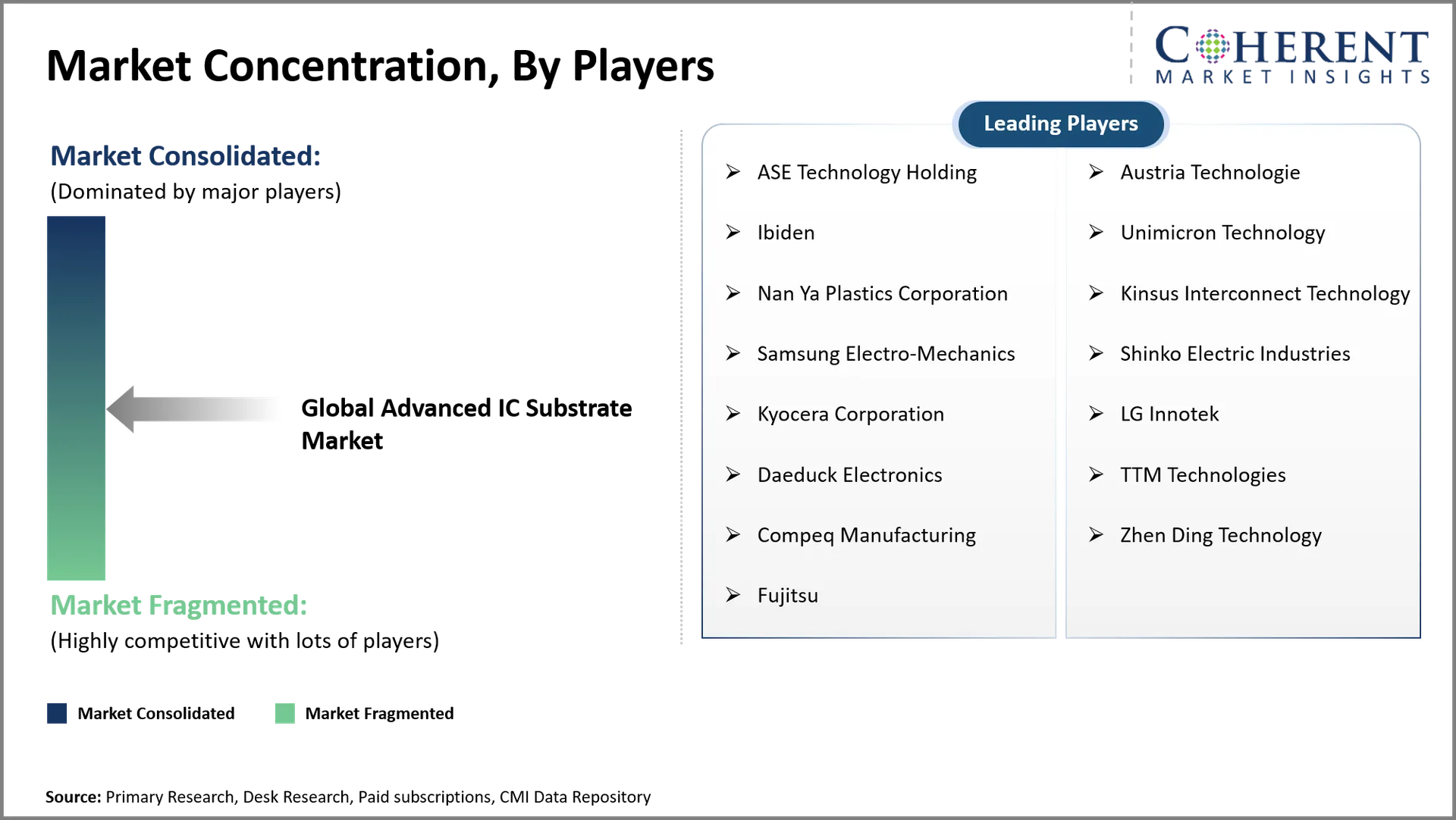
The global advanced IC substrate market is led by Ibiden, Unimicron Technology, Samsung Electro-Mechanics, Shinko Electric Industries, and Nan Ya Printed Circuit Board. These manufacturers compete through substrate miniaturization, production yields, high-density interconnections, and long-term customer relationships. Ibiden is expanding Japanese production capacity for artificial intelligence processors and application-specific integrated circuits. Samsung Electro-Mechanics announced a strategic partnership with NVIDIA on October 21, 2026, to deliver sophisticated substrates and dedicated production facilities in South Korea. Unimicron is enhancing Taiwanese manufacturing capacity for artificial intelligence computing needs. These approaches hinge on specialist engineering, reliable supply, and strong partnerships with leading chip designers.
Top Manufacturers and Notable Products in the Advanced IC Substrate Market
Manufacturer | Notable Product | Key features |
Ibiden Co., Ltd. | Flip-Chip Ball Grid Array substrates | High-density wiring, multilayer structures, and support for artificial intelligence processors and high-performance computing |
Unimicron Technology Corporation | Ajinomoto Build-up Film substrates | Fine-pitch interconnections, high wiring density, and support for advanced processor and networking packages |
Shinko Electric Industries Co., Ltd. | Flip-Chip package substrates | High-density interconnections, reliable electrical performance, and support for advanced semiconductor packaging |
Samsung Electro-Mechanics Co., Ltd. | Flip-Chip Ball Grid Array substrates | Fine circuit patterns, large package formats, and support for server processors and artificial intelligence accelerators |
AT&S | High-end integrated circuit substrates | Advanced multilayer designs, fine-line circuitry, and support for high-performance computing and networking applications |
Market Report Scope
Report Coverage | Details | ||
Base Year | 2025 | Market Size in 2026: | USD 18.00 Bn |
Historical Data For: | 2020 To 2024 | Forecast Period: | 2026 To 2033 |
Forecast Period 2026 To 2033 CAGR: | 8% | 2033 Value Projection: | USD 33.00 Bn |
Geographies covered: |
| ||
Segments covered: |
| ||
Companies covered: | ASE Technology Holding, Austria Technologie, Ibiden, Unimicron Technology, Nan Ya Plastics Corporation, Kinsus Interconnect Technology, Samsung Electro-Mechanics, Shinko Electric Industries, Kyocera Corporation, LG Innotek, Daeduck Electronics, TTM Technologies, Compeq Manufacturing, Zhen Ding Technology, Fujitsu | ||
Growth Drivers: |
| ||
Restraints & Challenges: |
| ||
Analyst Opinion (Expert Opinion)
- The industry's future will increasingly depend on substrates designed for artificial intelligence accelerators, high-bandwidth memory, and increasingly complex chiplet architectures. Larger packages will require improved warpage management, tighter circuit geometries, and stronger power delivery. Suppliers must also be ready for heterogeneous integration, where different dies need to be precisely electrically and thermally coordinated. The glass-core substrates could be strategically important once manufacturers demonstrate scalable production, dependable yields and cost-effective integration.
- Strongest market opportunities are for high-performance flip-chip ball grid array substrates for artificial intelligence servers and application-specific integrated circuits. Japan, Taiwan and South Korea have shown manufacturing capacity and integrated supply chains for semiconductors. The U.S. offers chances for suppliers that are supporting the domestic development of sophisticated packaging and diversification of the semiconductor supply chain. For processors, companies need to focus on high-density interconnections, large-format substrates and embedded passive components to meet the stringent requirements.
- Market participants should get long-term customer commitments before making costly capacity additions. Investments in sophisticated inspection, automated flaw detection, precision manufacturing and real-time process monitoring should be made to increase production yields. Working closely with chip designers, foundries and package providers in a strategic collaboration can assist align substrate specs to the chip architectures coming down the pipeline. Manufacturers should also diversify crucial material suppliers and qualify alternate production sites. Such techniques can improve supply reliability, maintain margins and increase competitiveness in technically challenging applications.
Speak to the analyst
Want personalized insights?
Take the findings above to one of our principal consultants, or have the report rebuilt around the segments, geographies and competitors you actually track.
Market Segmentation
- Substrate Type Insights (Revenue, USD Billion, 2021 - 2033)
- Flip Chip Ball Grid Array Substrates
- Flip Chip Chip Scale Package Substrates
- Fine-Pitch Ball Grid Array Substrates
- Others
- Technology Type Insights (Revenue, USD Billion, 2021 - 2033)
- High-Density Interconnect Substrates
- Build-Up Film Substrates
- Coreless Substrates
- Embedded Component Substrates
- Glass-Core Substrates
- Application Insights (Revenue, USD Billion, 2021 - 2033)
- Consumer Electronics
- High-Performance Computing
- Data Centers and Artificial Intelligence
- Automotive Electronics
- Telecommunications and Networking
- Industrial Electronics
- Regional Insights (Revenue, USD Billion, 2021 - 2033)
- North America
- U.S.
- Canada
- Latin America
- Brazil
- Argentina
- Mexico
- Rest of Latin America
- Europe
- Germany
- U.K.
- Spain
- France
- Italy
- Russia
- Rest of Europe
- Asia Pacific
- China
- India
- Japan
- Australia
- South Korea
- ASEAN
- Rest of Asia Pacific
- Middle East
- GCC Countries
- Israel
- Rest of Middle East
- Africa
- South Africa
- North Africa
- Central Africa
- North America
- Key Players Insights
- ASE Technology Holding
- Austria Technologie
- Ibiden
- Unimicron Technology
- Nan Ya Plastics Corporation
- Kinsus Interconnect Technology
- Samsung Electro-Mechanics
- Shinko Electric Industries
- Kyocera Corporation
- LG Innotek
- Daeduck Electronics
- TTM Technologies
- Compeq Manufacturing
- Zhen Ding Technology
- Fujitsu
Sources
Primary Research Interviews
- IC Substrate Manufacturers & Suppliers
- Semiconductor Packaging Engineers & Designers
- Electronics Component Distributors
- Data Center & Consumer Electronics OEMs
Magazines
- Semiconductor Digest
- Electronics Weekly
- IEEE Spectrum
- Printed Circuit Design & Fab (PCD&F)
Journals
- IEEE Transactions on Components, Packaging and Manufacturing Technology
- Journal of Electronic Materials
- Microelectronics Reliability
Associations
- IPC - Association Connecting Electronics Industries
- SEMI (Semiconductor Equipment and Materials International)
- Japan Electronics and Information Technology Industries Association (JEITA)
- Semiconductor Industry Association (SIA)
Public Domain Sources
- U.S. International Trade Commission (USITC)
- World Semiconductor Trade Statistics (WSTS)
- U.S. Department of Commerce - Bureau of Industry and Security (BIS)
- European Commission - Digital Industry Reports
Proprietary Elements
- CMI Data Analytics Tool
- Proprietary CMI Existing Repository of information for last 10 years
Get access to 250+ pages report
Every segment, forecast, competitor profile and data table behind the analysis above — available for instant download.
- ESOMAR Member
- ISO 9001:2015 Certified
- D-U-N-S Registered
- GDPR & CCPA Compliant
Frequently Asked Questions
The global advanced IC substrate market is expected to stand at USD 18.00 Bn in 2026 and is expected to reach USD 33.00 Bn by 2033.
The CAGR of the global advanced IC substrate market is projected to be 8% from 2026 to 2033.
Growing demand for AI accelerators and high-performance computing processors and Increasing adoption of chiplet architectures and advanced semiconductor packaging are the major factors driving the growth of the global advanced IC substrate market.
High capital expenditure for advanced substrate manufacturing facilities and Limited availability of advanced materials and specialized production equipment are the major factors hampering the growth of the global advanced IC substrate market.
In terms of substrate type, flip chip ball grid array substrates segment is estimated to dominate the market revenue share in 2026.
An advanced IC substrate provides electrical interconnections, mechanical support, and power distribution between semiconductor dies and printed circuit boards.
Chiplet architectures require precise interconnections between multiple semiconductor dies, increasing demand for sophisticated multilayer substrates.