

Global Glass Core Substrate Market Size and Forecast – 2026 To 2033
The global glass core substrate market is expected to grow from USD 130.0 Mn in 2026 to USD 1,042.0 Mn by 2033, registering a compound annual growth rate (CAGR) of 32% from 2026 to 2033. The global glass core substrate market is driven by rising chiplet architecture adoption. On May 26, 2026, Advanced Semiconductor Engineering, Inc. (ASE) announced the development of an industry-first automated 310mm × 310mm panel-level packaging production line, advancing its leadership in next-generation advanced packaging technologies.
Key Takeaways of the Global Glass Core Substrate Market
- The Glass Core Substrates segment is expected to account for 45.0% of the global glass core substrate market share in 2026. Growing advanced packaging complexity is driving the growth of the segment. In June 2026, Applied Materials introduced new deposition, chemical mechanical planarization, and metrology systems. The systems target advanced packaging processes for artificial intelligence chips. The portfolio addresses tighter tolerances, thinner dies, and increasingly complex three-dimensional stacks.
- The Through Glass segment is estimated to capture 41.0% of the market share in 2026. Increasing demand for larger package sizes is majorly driving the growth of the segment. In April 2026, Taiwan Semiconductor Manufacturing Company reported production of 5.5-reticle CoWoS packages. It is developing a 14-reticle version for future artificial intelligence systems.
- The 2.5D Packaging segment is estimated to capture 35.0% of the market share in 2026. Rising high bandwidth memory integration is majorly driving the growth of the segment. In September 2025, SK hynix completed HBM4 development and prepared its mass-production system. The company reported doubled bandwidth compared with its previous generation.
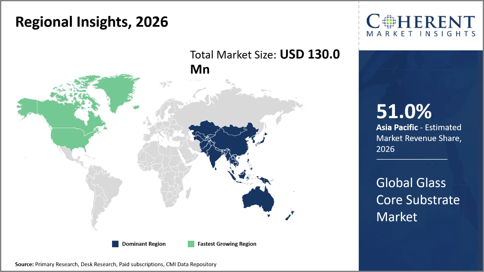
- Asia Pacific is expected to dominate the glass core substrate market in 2026 with a market share of 51.0%. Growing demand for panel-level packaging in Asia Pacific is driving the growth of the regional market. On May 8, 2026, Advanced Semiconductor Engineering, Inc. (ASE) and WUS Printed Circuit Co., Ltd. (WUS) announced a strategic collaboration for the construction of a state-of-the-art manufacturing facility in the Nanzih Technology Industrial Park, Kaohsiung, Taiwan. The two companies plan to jointly deploy resources to expand advanced manufacturing capacity that will reinforce Taiwan’s critical position in the global semiconductor value chain.
- North America is expected to account for 34.0% share in 2026 and is projected to record the fastest growth over the forecast period. Lower package warpage requirements in North America is driving the growth of the regional market. In September 2025, Intel Foundry presented a low thermal-gradient thermal compression bonding technology at the 2025 Electronics Components and Technology Conference. The process reduces temperature differences during bonding and lowers thermal expansion. Intel reported up to 45% lower thermal expansion than conventional bonding.
Segmental Insights
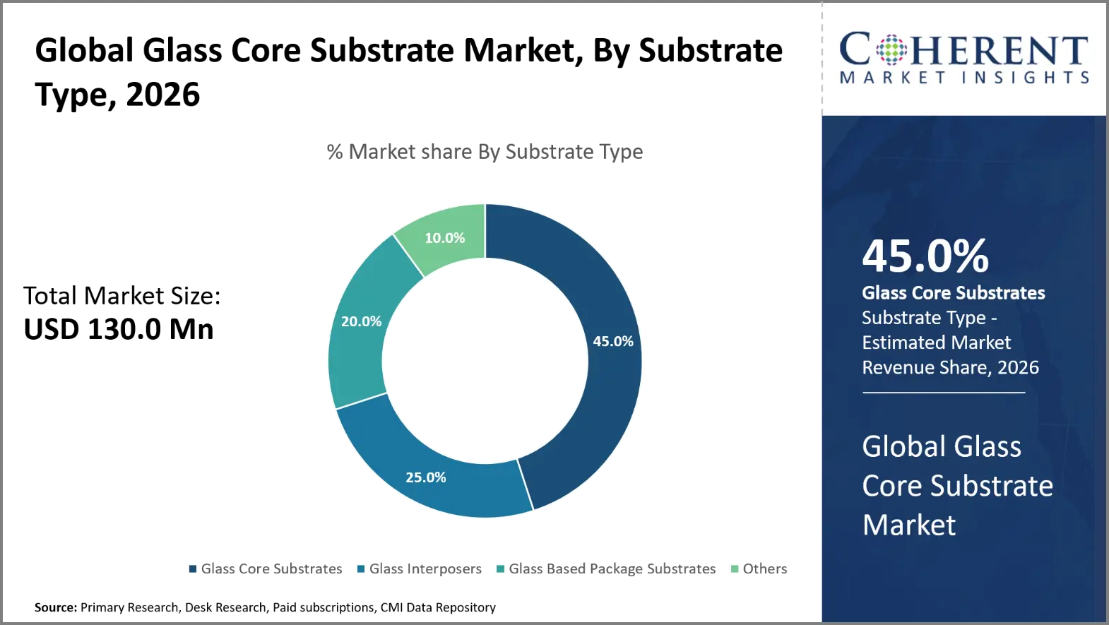
Why Does Glass Core Substrates Dominate the Global Glass Core Substrate Market?
The glass core substrates segment is expected to account for 45.0% of the global glass core substrate market share in 2026. Glass core substrates are popular because of their better dimensional stability for modern semiconductor packages. Low warpage helps to enable larger package sizes and tighter connection geometries. Glass also provides great surface flatness for denser redistribution layers. Its electrical insulation permits precise high density connecting architectures. These features support artificial intelligence processors, chiplets and high-performance computing packages. Glass can also be produced in greater package sizes without any equivalent dimensional distortions.
On August 25, 2026, AGC showcased glass substrates for advanced packaging at SEMICON India 2026. The company also displayed glass carriers for wafer and panel applications. Its portfolio targets semiconductor manufacturing processes requiring high dimensional precision.
- Current Industry Events of 2026
- Market Size Estimation
- Regional Breakdown
- Competitive Landscape
- Customer Intelligence
- Segmental Analysis
- Pricing Analysis
- Key Market Drivers, Challenges & Future Trends
- Customized Insights Section
Why is Through Glass the Most Crucial Technology Type?
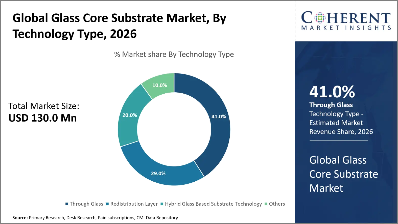
The through glass segment is expected to account for 41.0% of the global glass core substrate market share in 2026. Through-glass technology is significant because it enables vertical electrical interconnects through glass substrates. These interconnects provide shorter and more compact paths between semiconductor elements and packaging layers. Through-glass connection designs also enable the high interconnect densities required by modern chiplet systems. They can enhance signal integrity with complicated package designs. The method gives 3-D integration with the dimensional stability of glass. It also enables connectivity between package surfaces without traditional substrate topologies. Through-glass structures are therefore very essential for artificial intelligence and high-performance computer applications.
On May 22, 2025, Nippon Electric Glass Co., Ltd. developed two types of TGV (Through Glass Vias) glass core substrates for next-generation semiconductor package applications and has begun providing samples of both. The offered products include 515 x 510 mm substrates with TGV processed in-house, as well as unprocessed (TGV-free) mother glass.
2.5D Packaging Dominates the Global Glass Core Substrate Market
The 2.5D packaging segment is expected to account for 35.0% of the global glass core substrate market share in 2026. 2.5D packaging dominates because it combines multiple semiconductor components within a highly integrated package. This architecture places processors, memory, and other components alongside each other on an interposer. Glass provides dimensional stability needed for increasingly large 2.5D package structures. It also supports dense interconnects between chiplets and high-bandwidth memory devices. Artificial intelligence accelerators increasingly require this type of heterogeneous integration. Glass substrates can accommodate larger package dimensions while controlling warpage during manufacturing. Consequently, 2.5D packaging provides an important commercialization pathway for glass core substrates.
On September 16, 2026, Taiwan Semiconductor Manufacturing Company completed certification for 5.5-reticle CoWoS interposers. The company is expanding interposer sizes to integrate more advanced processors and high-bandwidth memory. Its roadmap directly addresses larger artificial intelligence packages requiring higher bandwidth and greater compute density.
Current Events and their Impact
Current Events | Description and its Impact |
U.S. CHIPS and Science Act |
|
European Chips Act 2.0 Proposal |
|
Glass Core Substrate Market Dynamics
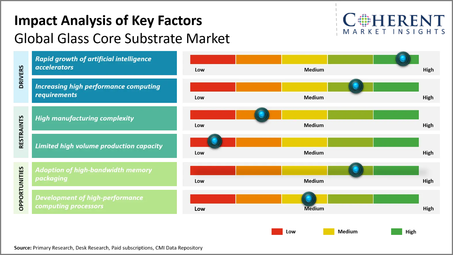
Market Drivers
Rapid growth of artificial intelligence accelerators
Accelerators for artificial intelligence that are rapidly growing are driving demand for sophisticated semiconductor packaging. The accelerators need larger packages with higher link densities and better electrical performance. Glass core substrates offer outstanding dimensional stability for these complicated package topologies. Their minimal warpage allows for bigger package sizes and finer interconnect topologies. The glass also supports dense through-glass connections between chiplets and memory components. These properties make glass substrates a good choice for artificial intelligence computers that require high bandwidth and efficient power delivery. Increasing artificial intelligence infrastructure investments are therefore encouraging semiconductor manufacturers to evaluate glass-based packaging solutions for next-generation accelerator designs.
On March 18, 2025, NVIDIA announced the next evolution of the NVIDIA Blackwell AI factory platform, NVIDIA Blackwell Ultra, paving the way for the age of AI reasoning. NVIDIA Blackwell Ultra boosts training and test-time scaling inference to enable organizations everywhere to accelerate applications such as AI reasoning, agentic AI and physical AI.
Increasing high performance computing requirements
Increasing high-performance computing requirements are driving semiconductor manufacturers toward larger and more sophisticated package architectures. High-performance processors increasingly integrate multiple chiplets, memory components, and specialized computing units within compact packages. Glass substrates provide high dimensional stability across large package areas. This feature contributes to control of warpage in sophisticated packaging techniques. Glass also allows to realize dense interconnect arrangements for high-bandwidth communication between integrated components. Better signal integrity can enable demanding computing workloads such as artificial intelligence, scientific computing and data analytics.
On October 13, 2025, OpenAI and Broadcom Inc. announced a collaboration for 10 gigawatts of custom AI accelerators. OpenAI will design the accelerators and systems, which will be developed and deployed in partnership with Broadcom. By designing its own chips and systems, OpenAI can embed what it’s learned from developing frontier models and products directly into the hardware, unlocking new levels of capability and intelligence.
Market Restraints/Challenges
- High Manufacturing Complexity: Fine-line patterning, metallization, through-glass connection construction, and precision glass processing are required for glass core substrates. Production faults such as cracking, dimensional variation or connection failures could result in increased production costs and limited consistent high-volume manufacturing yields.
- Limited Commercial Manufacturing Capacity: The manufacturing for glass core substrates is not as advanced as the manufacturing for standard organic substrates. Limited supplier capacity, long customer validation cycles, specialized equipment requirements, and complex process integration may prevent broad acceptance in advanced semiconductor packaging applications.
Emerging Trends
- Larger Glass Substrate Formats: To meet the needs of ever larger chip packages, manufacturers are working on larger glass substrates. Larger sizes may improve manufacturing efficiency, yet retain dimensional stability. This trend supports AI processors, high-performance computer systems, and sophisticated chiplet designs that require large packaging areas.
- Advanced Through-Glass Interconnects: Through-glass interconnect technologies are evolving to support higher density vertical electrical connections. Improved hole creation, metallization and dimensional control allow finer connection pitches. These advancements further demonstrate the potential of glass substrates for high-bandwidth memory, chiplets and complicated heterogeneous packaging.
- Integration With 2.5D Packaging: Glass substrates are increasingly being considered for 2.5D package topologies combining CPUs, memory and chiplets. Glass supports large interposers with numerous interconnections due to flatness and dimensional stability. This trend is driving acceptance across artificial intelligence and high-performance computing applications.
- Development Of Glass Manufacturing Ecosystems: Semiconductor manufacturers are partnering with glass manufacturers, packaging businesses and equipment providers. The collaborations span material processing, through-glass interconnects, metallization and package integration. Such ecosystem growth can speed up qualification and commercial manufacturing of glass substrates.
Regional Insights
Why is Asia Pacific a Strong Market for Glass Core Substrate?
Asia Pacific is expected to account for a market share of 51.0% in 2026. Asia Pacific benefits from dense semiconductor packaging ecosystems across Taiwan, South Korea, Japan, and China. Taiwan Semiconductor Manufacturing Company is developing large-panel packaging capabilities for artificial intelligence processors. South Korean companies are advancing pilot production and commercial qualification. Japanese suppliers contribute precision glass, packaging materials, and high-density processing expertise. Dai Nippon Printing began phased operations for a TGV glass-core pilot line in Saitama in December 2025. Its substrates measure 510 × 515 millimeters. The company plans sample shipments from early 2026. These developments create close integration between glass processing, substrate manufacturing, foundry packaging, and artificial intelligence chip production.
Why Does North America Glass Core Substrate Market Exhibit High Growth?
North America is expected to register the fastest growth with a CAGR of 32.7% over the forecast period. North America is projected to account for 34.0% of the global glass core substrate market in 2026. North America is advancing glass core substrates through domestic advanced-packaging programs and artificial intelligence infrastructure. Absolics received substantial U.S. government support for its Covington, Georgia manufacturing facility. The facility focuses on glass substrates for artificial intelligence, high-performance computing, and data-center chips. The United States Department of Commerce announced UD 100 million for Absolics through the National Advanced Packaging Manufacturing Program. Intel is also developing glass substrates for large artificial intelligence packages and high-performance computing systems. Intel demonstrated glass technology supporting larger package formats and denser interconnect architectures. These initiatives are creating a domestic qualification ecosystem connecting substrate developers, chip designers, packaging companies, and research institutions.
Global Glass Core Substrate Market Outlook for Key Countries
Why is China Emerging as a Major Hub in the Glass Core Substrate Market?
China is strengthening domestic glass-substrate capabilities alongside its broader semiconductor packaging development. Domestic companies are exploring glass cores for advanced package architectures requiring larger areas and improved dimensional stability. The country's extensive display-glass manufacturing base provides relevant experience in large-area glass handling and precision processing. Chinese semiconductor packaging companies can leverage this manufacturing foundation for glass-core development. Demand is also supported by domestic artificial intelligence accelerator development and growing advanced-packaging requirements. Localized substrate development is particularly important because high-end package substrates remain concentrated among Asian suppliers.
Is U.S. the Next Growth Engine for the Glass Core Substrate Market?
The U.S. glass core substrate market is being shaped strongly by Intel and Absolics. Intel has researched glass substrates for more than a decade and targets large packages for artificial intelligence and data-center workloads. Its technology can enable substantially higher interconnect density than conventional packaging materials. Absolics is developing its glass-core packaging ecosystem in Covington, Georgia. The U.S. Department of Commerce awarded Absolics USD 100 million under the National Advanced Packaging Manufacturing Program. Earlier funding supported a 120,000-square-foot manufacturing facility. These investments connect glass substrate production with domestic advanced-packaging research, customer qualification, artificial intelligence accelerators, and high-performance computing systems.
Taiwan Glass Core Substrate Market Analysis and Trends
Taiwan is benefiting from its concentration of advanced foundries, substrate manufacturers, and packaging specialists. Taiwan Semiconductor Manufacturing Company is developing large-area packaging architectures for artificial intelligence processors. Taiwan's advanced packaging ecosystem provides direct access to demanding chiplet and high-bandwidth memory requirements. Local substrate manufacturers are also evaluating glass cores for future high-density packages. Customer qualification can progress efficiently because substrate development occurs near major semiconductor fabrication and packaging operations. Taiwan's strength in chiplet integration therefore creates a distinct adoption pathway for glass substrates. The country's expertise in advanced packaging also supports experimentation with larger package formats and increasingly complex heterogeneous computing architectures.
Japan Glass Core Substrate Market Analysis and Trends
Japan has a distinct advantage from its combination of specialty glass expertise and semiconductor packaging capabilities. Dai Nippon Printing launched a TGV glass-core pilot line at its Kuki Plant in Saitama. Its 510 × 515-millimeter substrates target large-area semiconductor packages and high-density interconnects. Shinko Electric Industries has also demonstrated a 22-layer glass structure with eleven copper wiring layers on each side. Japanese suppliers are additionally developing glass materials, precision processing, and packaging technologies. Dai Nippon Printing plans to establish infrastructure for full mass production by fiscal year 2028. These developments position Japan strongly in high-layer-count substrates and precision glass-core manufacturing.
South Korea Glass Core Substrate Market Analysis and Trends
South Korea is rapidly moving glass core substrates from research toward commercial production. Samsung Electro-Mechanics established a pilot line at Sejong and has been preparing customer samples. In July 2026, Samsung Electro-Mechanics formed GlaSSEM with Dongwoo Fine-Chem for glass-core manufacturing. The joint venture targets production during the second half of 2027. LG Innotek is also developing glass substrates at its Gumi facility. Absolics, affiliated with South Korea's SKC, operates its glass-substrate manufacturing facility in Georgia. This combination gives South Korea expertise across materials, substrate manufacturing, electronics packaging, and customer qualification. South Korean memory and artificial intelligence hardware ecosystems further strengthen domestic glass-substrate development.
Global Glass Core Substrate Market - Glass Substrate Yield Improvement by Manufacturing Process
Manufacturing Process | Yield Improvement Indicator | Key Yield Benefit |
Laser Modification and Etching | Up To 35% Alignment Accuracy Improvement | Smaller TGVs And Narrower Pitches |
CO₂ Laser Processing | Fewer Processing Steps | Reduced Process Complexity and Faster Via Formation |
TGV Copper Filling | ±10% TGV Resistance Variation | Stable Electrical Interconnections |
Edge Coating | Reduced Glass Cracking After 260°C Reflow | Improved Dicing and Thermal Reliability |
Large-Panel Glass Processing | More Than 50% Warpage Reduction | Improved Alignment and Package Assembly |
How is Adoption of High-Bandwidth Memory Packaging Creating New Growth Opportunities in the Glass Core Substrate Market?
High-bandwidth memory packaging is creating opportunities for glass substrates because artificial intelligence accelerators require increasingly dense processor-memory connections. High-bandwidth memory stacks generate demanding interconnect requirements within large 2.5D and 3D packages. Glass offers exceptional dimensional stability, enabling larger interposers to maintain alignment across dense connection arrays. Its low warpage becomes particularly valuable as package dimensions increase around multiple high-bandwidth memory stacks. Glass also supports fine redistribution structures and through-glass connections for complex heterogeneous packages. Intel has demonstrated glass-substrate architectures targeting large artificial intelligence packages. Taiwan Semiconductor Manufacturing Company is developing advanced packaging approaches for artificial intelligence hardware, strengthening potential demand for larger glass-based interposers.
On February 12, 2026, Samsung Electronics announced that it has begun mass production of its industry-leading HBM4 and has shipped commercial products to customers. This achievement marks a first in the industry, securing an early leadership position in the HBM4 market.
Market Players, Key Development, and Competitive Landscape
Key Developments
- On July 6, 2026, SHINKO ELECTRIC INDUSTRIES CO., LTD. announced that its presentation at the 2025 IEEE 75th Electronic Components and Technology Conference (ECTC 2025), held in Dallas, Texas, U.S., was awarded the Outstanding Session Paper as part of the ECTC 2025 Best Paper Awards. This honor reflects the high recognition of the company’s research on glass core substrates.
- On December 16, 2025, TOPPAN Inc. announced it will install a pilot line to conduct research and development of advanced semiconductor packaging at the Ishikawa Plant in Japan acquired in 2023, aiming to commission the line in July 2026.
- On December 1, 2025, AGC announced it will showcase glass carriers for advanced packaging, glass substrates with microvias for glass core applications, films used in semiconductor manufacturing processes and production equipment, resin products, and more at SEMICON Japan 2025.
Competitive Landscape
The competitive landscape is shifting toward partnerships combining glass processing with advanced packaging expertise. Intel Corporation is developing glass substrates for large artificial intelligence and high-performance computing packages. Its technology targets higher interconnect density, improved power delivery, and larger package dimensions. In July 2026, Intel Corporation partnered with Lens Technology for precision glass processing and scalable manufacturing. Dai Nippon Printing launched a 510 × 515-millimeter TGV pilot line in Japan. It plans sample shipments from early 2026 and mass-production preparation for fiscal year 2028. Nippon Electric Glass developed its 515 × 510-millimeter GC Core for large advanced packages. Samsung Electronics is pursuing large-area 2.5D packaging through its H-Cube architecture with Samsung Electro-Mechanics and Amkor Technology.
Top Manufacturers and Notable Products
Manufacturer | Notable Product | Key features |
AGC | TGV Glass Substrate for Advanced Packaging | 510 × 515 mm panels, 20-150 μm via diameter, high aspect ratio up to 20:1, adjustable CTE, fine-pitch TGV formation |
Absolics | inProut Glass Substrate | Ultra-fine interconnections, embedded devices, AI-driven yield control, fine-pitch die interconnects, high-density packaging |
Nippon Electric Glass | Large TGV Glass Core Substrate | 515 × 510 mm format, laser modification and etching, CO₂ laser processing, fine vias, narrow-pitch interconnections |
Dai Nippon Printing | TGV Glass Core Substrate | 510 × 515 mm format, filled and conformal TGV structures, high flatness, dimensional stability, large-panel processing |
TOPPAN | TGV Glass Substrate | TGV formation with cavities, glass-core FC-BGA integration, glass interposer applications, advanced glass processing |
Market Report Scope
Report Coverage | Details | ||
Base Year | 2025 | Market Size in 2026: | USD 130.0 Mn |
Historical Data For: | 2020 To 2024 | Forecast Period: | 2026 To 2033 |
Forecast Period 2026 To 2033 CAGR: | 32% | 2033 Value Projection: | USD 1042.0 Mn |
Geographies covered: |
| ||
Segments covered: |
| ||
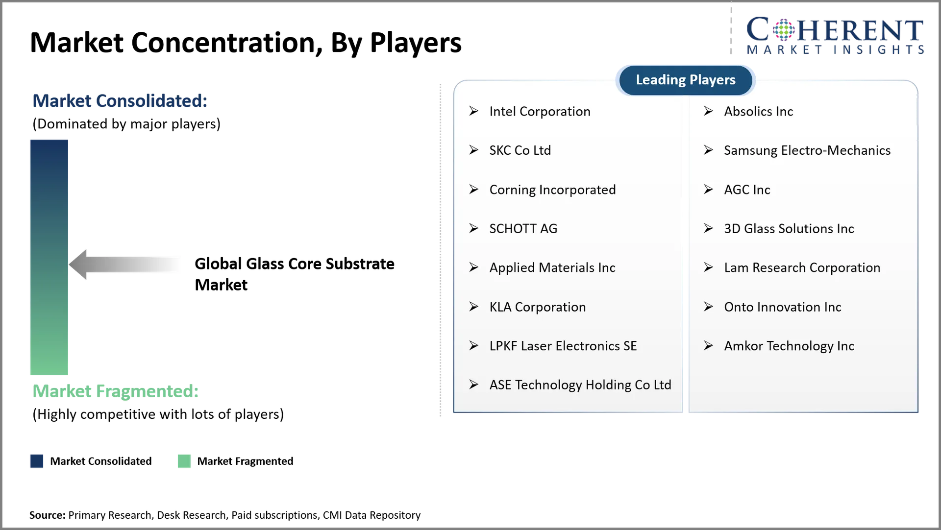
Companies covered: | Intel Corporation, Absolics Inc, SKC Co Ltd, Samsung Electro-Mechanics, Corning Incorporated, AGC Inc, SCHOTT AG, 3D Glass Solutions Inc, Applied Materials Inc, Lam Research Corporation, KLA Corporation, Onto Innovation Inc, LPKF Laser Electronics SE, Amkor Technology Inc, ASE Technology Holding Co Ltd | ||
Growth Drivers: |
| ||
Restraints & Challenges: |
| ||
Analyst Opinion (Expert Opinion)
- The industry is likely to move toward glass substrates as package dimensions continue expanding. Artificial intelligence accelerators will remain the strongest initial application. High-bandwidth memory integration will intensify requirements for stable, large-area packaging platforms. Glass should gain traction where organic substrates face warpage and dimensional limitations. Intel Corporation's focus on large packages demonstrates this transition toward glass-based architectures.
- The strongest opportunity should emerge in large-panel glass cores supporting 2.5D artificial intelligence packages. Japan, South Korea, Taiwan, and the U.S. should remain important development centers. Japan offers specialized glass expertise and large-panel development capabilities. South Korea combines substrate expertise with strong memory and packaging ecosystems. Taiwan offers proximity to advanced foundries and complex packaging operations.
- Players should prioritize reliable TGV formation, high-density metallization, large-panel handling, and automated inspection. Partnerships with glass processors can shorten the path toward scalable manufacturing. Companies should also qualify substrates directly with artificial intelligence accelerator and high-bandwidth memory package designers. Intel Corporation's collaboration with Lens Technology illustrates this partnership-led strategy. Manufacturers should develop both filled and conformal TGV structures for different package requirements. Dai Nippon Printing already plans both approaches in its pilot production.
Speak to the analyst
Want personalized insights?
Take the findings above to one of our principal consultants, or have the report rebuilt around the segments, geographies and competitors you actually track.
Market Segmentation
- Substrate Type Insights (Revenue, USD Million, 2021 - 2033)
- Glass Core Substrates
- Glass Interposers
- Glass Based Package Substrates
- Others
- Technology Type Insights (Revenue, USD Million, 2021 - 2033)
- Through Glass
- Redistribution Layer
- Hybrid Glass Based Substrate Technology
- Others
- Package Type Insights (Revenue, USD Million, 2021 - 2033)
- 2.5D Packaging
- 3D Packaging
- Chiplet Based Packaging
- Fan Out Packaging
- System In Package
- Others
- Application Insights (Revenue, USD Million, 2021 - 2033)
- AI and High-Performance Computing
- Data Center and Networking
- Co Packaged Optics
- 5G and 6G High Frequency Communication
- Automotive Electronics
- Consumer Electronics
- Others
- End User Insights (Revenue, USD Million, 2021 - 2033)
- Semiconductor Manufacturers and Foundries
- Outsourced Semiconductor Assembly and Test Companies
- Integrated Device Manufacturers
- Advanced Semiconductor Packaging Companies
- AI and High Performance Computing Chip Manufacturers
- Others
- Regional Insights (Revenue, USD Million, 2021 - 2033)
- North America
- U.S.
- Canada
- Latin America
- Brazil
- Argentina
- Mexico
- Rest of Latin America
- Europe
- Germany
- U.K.
- Spain
- France
- Italy
- Russia
- Rest of Europe
- Asia Pacific
- China
- India
- Japan
- Australia
- South Korea
- ASEAN
- Rest of Asia Pacific
- Middle East
- GCC Countries
- Israel
- Rest of Middle East
- Africa
- South Africa
- North Africa
- Central Africa
- North America
- Key Players Insights
- Intel Corporation
- Absolics Inc
- SKC Co Ltd
- Samsung Electro-Mechanics
- Corning Incorporated
- AGC Inc
- SCHOTT AG
- 3D Glass Solutions Inc
- Applied Materials Inc
- Lam Research Corporation
- KLA Corporation
- Onto Innovation Inc
- LPKF Laser Electronics SE
- Amkor Technology Inc
- ASE Technology Holding Co Ltd
Sources
Primary Research Interviews
- Semiconductor Packaging Engineers & Manufacturers
- Glass Substrate Material Suppliers & Distributors
- PCB (Printed Circuit Board) Manufacturers
- Electronics OEM & ODM Companies
Magazines
- Semiconductor Digest
- Electronic Design Magazine
- PCB Design & Fabrication Magazine
- Advanced Packaging Magazine
Journals
- Journal of Electronic Materials (Springer)
- IEEE Transactions on Components, Packaging and Manufacturing Technology
- Journal of Microelectronics and Electronic Packaging
Associations
- IPC - Association Connecting Electronics Industries
- Semiconductor Industry Association (SIA)
- Japan Electronics and Information Technology Industries Association (JEITA)
- International Electronics Manufacturing Initiative (iNEMI)
Public Domain Sources
- U.S. Securities and Exchange Commission (SEC) Filings
- World Semiconductor Trade Statistics (WSTS)
- U.S. Department of Commerce – International Trade Administration
- European Commission – Digital Industry Reports
Proprietary Elements
- CMI Data Analytics Tool
- Proprietary CMI Existing Repository of Information for Last 10 Years
Get access to 250+ pages report
Every segment, forecast, competitor profile and data table behind the analysis above — available for instant download.
- ESOMAR Member
- ISO 9001:2015 Certified
- D-U-N-S Registered
- GDPR & CCPA Compliant
Frequently Asked Questions
The global glass core substrate market is expected to stand at USD 130.0 Mn in 2026 and is expected to reach USD 1,042.0 Mn by 2033.
The CAGR of the global glass core substrate market is projected to be 32% from 2026 to 2033.
Rapid growth of artificial intelligence accelerators and Increasing high performance computing requirements are the major factors driving the growth of the global glass core substrate market.
High manufacturing complexity and Limited high volume production capacity are the major factors hampering the growth of the global glass core substrate market.
In terms of substrate type, glass core substrates segment is estimated to dominate the market revenue share in 2026.
A glass core substrate uses a glass layer as the structural foundation for advanced semiconductor packaging.
Glass maintains greater dimensional stability during processing, helping control deformation across large package structures.