Global Advanced Chip Packaging Market Size and Forecast – 2026-2033
The Global Advanced Chip Packaging Market is estimated to be valued at USD 53.90 billion in 2026 and is expected to reach USD 86.56 billion by 2033, exhibiting a compound annual growth rate (CAGR) of 7.0% from 2026 to 2033.
Key Takeaways of the Global Advanced Chip Packaging Market:
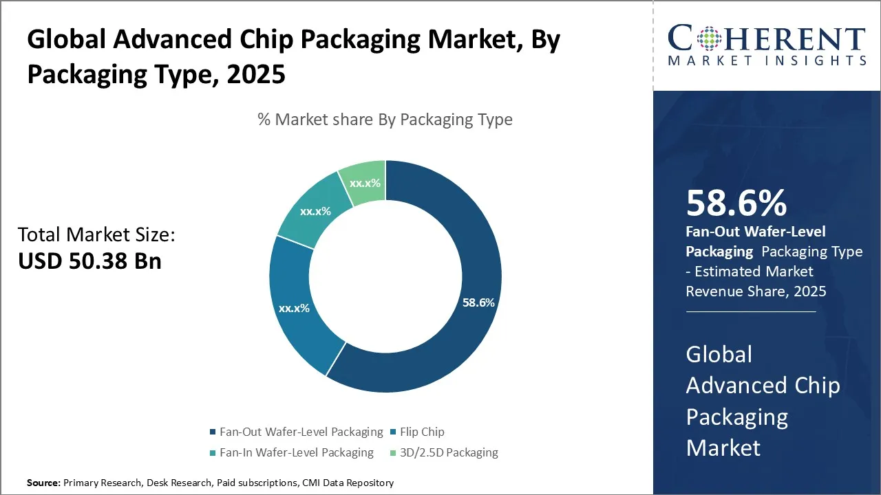
- The fan-out wafer-level packaging segment is expected to lead the market holding an estimated share of 59.6% in 2026.
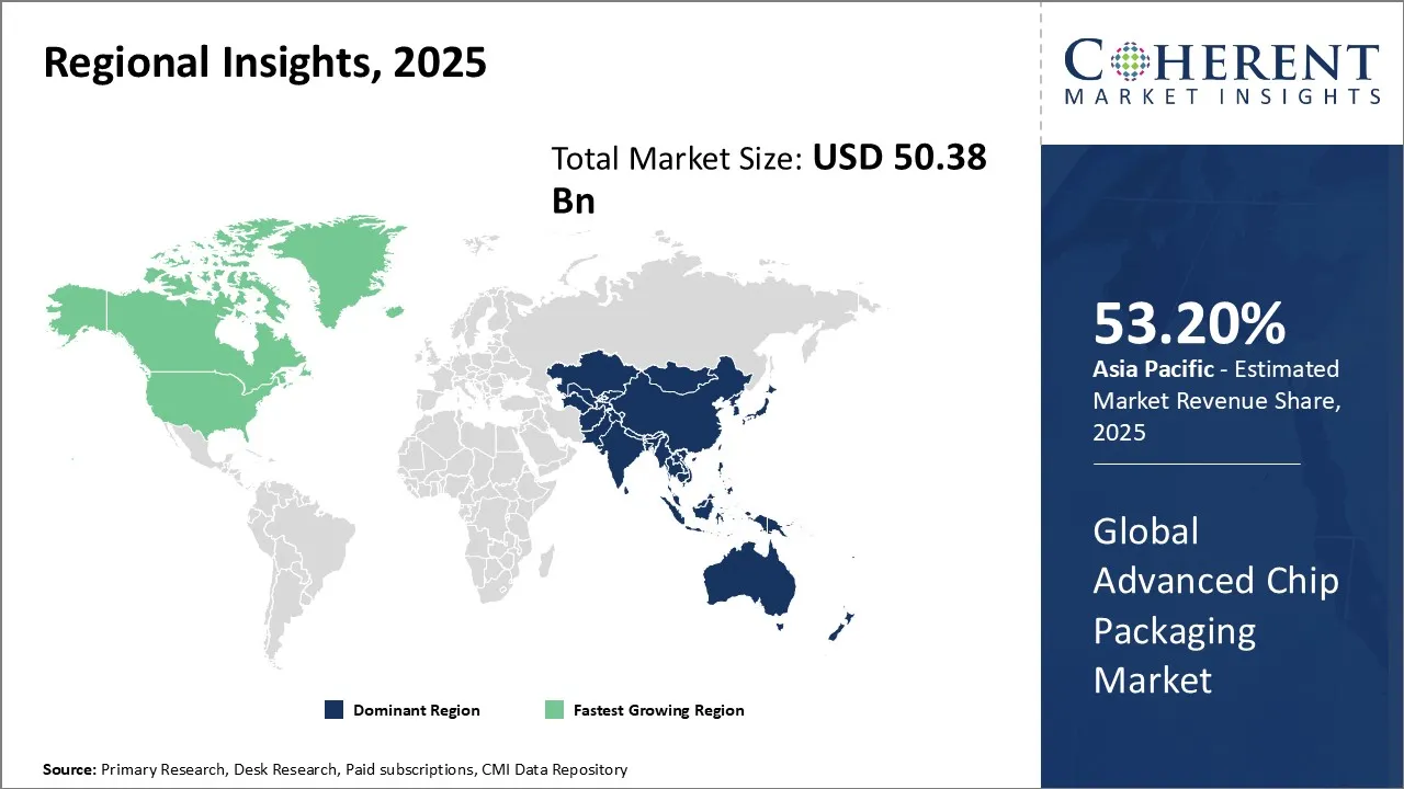
- Asia Pacific is estimated to lead the market with a share of 53. 2% in 2026.
- North America, holding a share of 29. 3% in 2026, is projected to be the fastest growing region.
Market Overview:
The market trend for the advanced chip packaging market is driven by the increasing demand for smaller, faster, and more efficient electronic devices. The need for high-performance computing, 5G networks, and the Internet of Things (IoT) is fueling the growth of this market. Additionally, the rising adoption of advanced packaging technologies, such as 2.5D and 3D packaging, will add to the market growth during the forecast period.
Current Events and their Impact:
|
Current Events |
Description and its impact |
|
Escalating U.S.-China Chip Trade Restrictions |
|
|
Technological Innovation in Advanced Chip Packaging Technologies |
|
Uncover macros and micros vetted on 75+ parameters: Get instant access to report
Global Advanced Chip Packaging Market Insight, by Packaging Type – Increasing Adoption of Advanced Semiconductor Packaging in High-Performance Applications Drives Fan-Out Wafer-Level Packaging Segment Growth
Fan-out wafer-level packaging segment is expected to contribute the highest share of 59.6% in the market in 2026. Fan-Out Wafer-Level Packaging (FOWLP) is a cutting-edge packaging solution that makes possible the integration of multiple dies and passive components into a single package, resulting in reduced package size and enhanced thermal management.
The growing demand for high-performance, low-power, and compact semiconductor devices in different applications, such as smartphones, wearables, automotive electronics, and IoT devices, is greatly adding to segment growth. FOWLP technology helps create highly integrated and miniaturized packages, making it suited for applications where space is limited.
Moreover, the increasing adoption of 5G technology and the proliferation of connected devices are creating demand for FOWLP solutions. 5G devices need advanced packaging technologies, such as FOWLP, to support higher data rates and increased bandwidth. Also, FOWLP technology makes possible the integration of different die technologies, such as logic, memory, and analog, into a single package, thereby facilitating the development of highly integrated and multifunctional devices.
Role of Artificial Intelligence (AI) in the Market:
Artificial Intelligence (AI) is playing a pivotal role in revolutionizing the advanced chip packaging market by enabling smarter design, automation, and defect detection throughout the packaging lifecycle. AI algorithms are being integrated into electronic design automation (EDA) tools to optimize layout planning for chiplets, reduce thermal bottlenecks, and predict stress points in 2.5D and 3D packaging structures. These tools enhance yield rates and reduce time-to-market by simulating complex interconnects and thermal profiles in real time. In manufacturing, AI-driven process control is being used to monitor wafer bonding, lithography alignment, and bump formation with greater accuracy than traditional systems.
A notable instance of AI’s impact is seen in ASE Technology’s deployment of machine learning models to predict and correct wafer warpage during the fan-out packaging process. By training models on historical production data, ASE reduced material waste by over 20% and significantly improved die-attach yield rates.
Regional Insights:
To learn more about this report, Download Free Sample
Asia Pacific Advanced Chip Packaging Market Analysis and Trends
Asia Pacific, holding a share of 53.2% in 2026, is expected to dominate the global advanced chip packaging market. The region boasts a robust semiconductor industry, with countries like China, South Korea, Taiwan, and Japan being major players in chip manufacturing and packaging. The presence of leading foundries, such as TSMC and Samsung, along with advanced packaging solution providers, has created a strong ecosystem for advanced chip packaging in the region.
Moreover, government initiatives and investments in the semiconductor sector have further fueled the growth of advanced chip packaging in Asia Pacific. For instance, China's "Made in China 2026" plan aims to bolster the domestic semiconductor industry, while South Korea and Taiwan have implemented policies to maintain their leadership in semiconductor manufacturing.
North America Advanced Chip Packaging Market Analysis and Trends
North America, holding a share of 29.3% in 2026, is expected to exhibit the fastest growth in the global advanced chip packaging market. The region's growth can be ascribed to the presence of major technology companies, such as Intel, AMD, and Nvidia, which are driving innovation in chip packaging technologies. The increasing adoption of artificial intelligence, IoT, and 5G technologies in various industries, such as automotive, healthcare, and aerospace, has further propelled the demand for advanced chip packaging solutions in North America. Additionally, the region's focus on miniaturization and the development of high-performance computing systems has fueled the growth of advanced chip packaging technologies such as 2.5D and 3D packaging.
Global Advanced Chip Packaging Market Outlook for Key Countries:
U.S. Advanced Chip Packaging Market Analysis and Trends
The U.S. advanced chip packaging market is driven by the presence of major semiconductor companies and a strong focus on innovation. Intel, a key player in the market, has been actively investing in advanced packaging technologies, such as Foveros and EMIB, to enable the development of high-performance processors. AMD has also made significant strides in advanced packaging with its chiplet-based designs, which allow for the integration of multiple chips in a single package. The U.S. government's support for the semiconductor industry, through initiatives like the CHIPS for America Act, is expected to further boost the growth of advanced chip packaging in the country.
China Advanced Chip Packaging Market Analysis and Trends
China advanced chip packaging market benefits from the country's goals to become self-sufficient in semiconductor technology. The "Made in China 2026" initiative has been put in place to increase domestic production of semiconductors and advanced packaging solutions. Chinese companies, such as JCET and TFME, are expanding their advanced packaging capabilities to fulfil the growing demand from the domestic market.
Taiwan Advanced Chip Packaging Market Analysis and Trends
Taiwan continues to lead in the advanced chip packaging market, due to the presence of TSMC, the world's largest foundry. TSMC is leading the development of advanced packaging technologies, offering solutions like Integrated Fan-Out (InFO) and Chip-on-Wafer-on-Substrate (CoWoS). The company works closely with its customers to provide end-to-end solutions. Taiwan has a well-established semiconductor ecosystem, which is responsible for its leadership in the advanced chip packaging market.
South Korea Advanced Chip Packaging Market Analysis and Trends
South Korea advanced chip packaging market benefits from the presence of Samsung, who is a global leader in semiconductor manufacturing and packaging. The company invests heavily in advanced packaging technologies, such as X-Cube and I-Cube, to help develop high-performance and low-power devices. The company has a vertically integrated structure, including chip design, manufacturing, and packaging. This structure helps the company maintain its dominance in the market.
Market Players, Key Development, and Competitive Intelligence:
To learn more about this report, Download Free Sample
Key Developments:
- In May 2025, TSMC, a semiconductor contract manufacturing and design company, announced plans to open a chip design center in Munich, Germany. TSMC currently has nine other chip design centers across the world, located in Canada, China, Japan, Taiwan, and the U.S., but the Munich facility will be the company's first in Europe.
- In February 2025, Advanced Semiconductor Engineering, Inc. (ASE), a member of ASE Technology Holding Co., Ltd., launched its fifth plant in Penang, Malaysia. The new plant is part of a strategic expansion plan that will expand the floor space of ASE’s Malaysia facility from its current area of 1 million square feet to approximately 3.4 million square feet.
- In January 2024, Amkor Technology, Inc., a provider of semiconductor packaging and test services, and GlobalFoundries (GF), a global semiconductor manufacturer, partnered to strengthen semiconductor manufacturing in Europe. To facilitate this collaboration, GF transferred its 300 mm Bump (12-inch bump, CuP and plated bump) and Sort lines from its Dresden site to Amkor’s IATF 16949 certified Porto plant to establish the first at-scale back-end facility in Europe.
- In November 2022, Lam Research Corp., a supplier of wafer-fabrication equipment, acquired SEMSYSCO GmbH, a global provider of wet processing semiconductor equipment, from Gruenwald Equity and other investors. With the addition of SEMSYSCO, Lam gained capabilities in advanced packaging, ideal for leading-edge logic chips.
Top Strategies Followed by Global Advanced Chip Packaging Market Players
- Established players are investing heavily in R&D to develop cutting-edge technologies that can meet the ever-increasing demands of the industry.
- For instance, Intel Corporation is investing in advanced packaging technologies such as 3D stacking and silicon interposers to improve the performance of their chips.
- Mid-level players are investing in cost-effective manufacturing processes and materials to reduce production costs while maintaining product quality.
- Micropack has adopted the double-mask etching technique to produce high-quality Gas Electron Multiplier (GEM) foils domestically to reduce reliance on imports and offering budget-friendly solutions.
- Small-scale players are targeting niche markets with unique features or innovative products.
- Pragmatic Semiconductor is carving out a niche in the advanced chip packaging market by producing ultra-thin, flexible chips suitable for embedding in everyday items. Their "fab-in-a-box" model allows for modular and automated production lines, making semiconductor manufacturing more accessible and adaptable.
Market Report Scope
Advanced Chip Packaging Market Report Coverage
| Report Coverage | Details | ||
|---|---|---|---|
| Base Year: | 2025 | Market Size in 2026: | USD 53.90 Bn |
| Historical Data for: | 2020 To 2024 | Forecast Period: | 2026 To 2033 |
| Forecast Period 2026 to 2033 CAGR: | 7.0% | 2033 Value Projection: | USD 86.56 Bn |
| Geographies covered: |
|
||
| Segments covered: |
|
||
| Companies covered: |
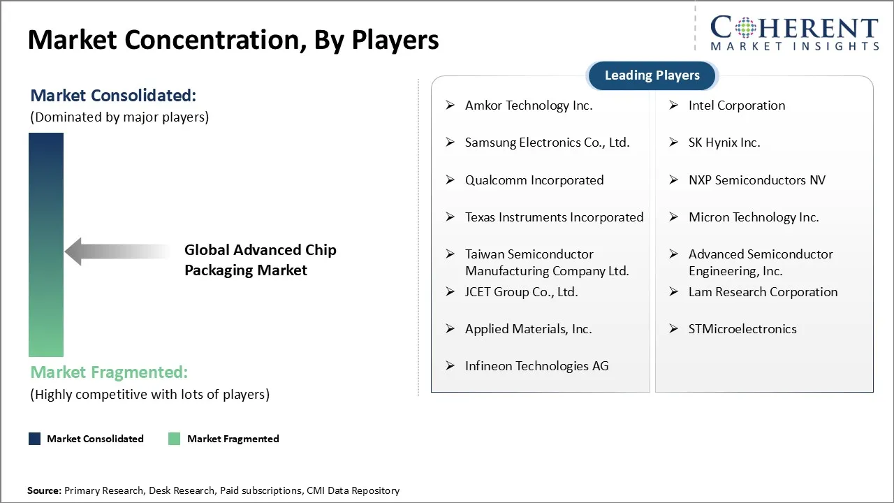
Amkor Technology Inc., Intel Corporation, Samsung Electronics Co., Ltd., SK Hynix Inc., Qualcomm Incorporated, NXP Semiconductors NV, Texas Instruments Incorporated, Micron Technology Inc., Taiwan Semiconductor Manufacturing Company Ltd., Advanced Semiconductor Engineering, Inc., JCET Group Co., Ltd., Lam Research Corporation, Applied Materials, Inc., STMicroelectronics, and Infineon Technologies AG |
||
| Growth Drivers: |
|
||
| Restraints & Challenges: |
|
||
Uncover macros and micros vetted on 75+ parameters: Get instant access to report
Market Dynamics
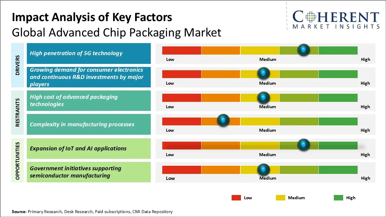
To learn more about this report, Download Free Sample
Global Advanced Chip Packaging Market Driver - High penetration of 5G technology
As 5G networks continue to expand and gain traction worldwide, there is an increasing demand for advanced chip packaging solutions that can support the high-speed, low-latency, and enhanced connectivity requirements of 5G devices and infrastructure. Advanced chip packaging techniques, such as 2.5D and 3D packaging, make possible the integration of multiple chips and components within a single package, offering improved performance and miniaturization. These packaging solutions are crucial for the development of 5G-enabled devices including smartphones, tablets, IoT devices, and network equipment.
Samsung's Galaxy S20 series uses Exynos 990 System-on-Chip (SoC). This SoC employs a three-dimensional (3D) package-on-package (PoP) design with flip-chip interconnects (fcPoP), integrating the SoC and memory devices within a single package.
Global Advanced Chip Packaging Market Opportunity - Expansion of IoT and AI applications
The proliferation of connected devices and the growing demand for smart systems across various sectors, such as automotive, healthcare, industrial automation, and consumer electronics, are driving the need for advanced packaging solutions. IoT devices require compact, power-efficient, and high-performance chips to enable seamless connectivity and data processing. Advanced packaging technologies, such as system-in-package (SiP) and fan-out wafer-level packaging (FOWLP), offer the necessary miniaturization, integration, and functionality to meet the demands of IoT applications.
Similarly, AI applications, including machine learning and deep learning, rely on advanced chip packaging to deliver the required computing power and bandwidth. The integration of multiple chips, such as processors, memory, and sensors, in a single package enables the development of high-performance AI systems. For instance, Broadcom has introduced a 3.5D Extended Data Scale in Package (XDSiP) technology aimed at enhancing AI chip interconnectivity.
Analyst Opinion (Expert Opinion):
- The push toward higher performance and energy efficiency in AI, HPC, and mobile applications is accelerating the adoption of 2.5D and 3D chip stacking. These architectures enable integration of multiple chiplets with different functionalities in a single package, reducing latency and power consumption — a game-changer for future computing.
- As thinner, high-performance form factors become standard in smartphones and edge AI devices, Fan-Out Wafer-Level Packaging (FO-WLP) offers an ideal balance between performance, footprint, and thermal efficiency. This trend will dominate next-gen SoCs and RF modules.
- Emerging materials like glass substrates and hybrid bonding are unlocking finer pitch interconnects and better thermal characteristics. These breakthroughs are crucial to overcoming the bottlenecks in high-density integration and will define competitiveness in the AI and 5G era.
Market Segmentation
- Packaging Type Insights (Revenue, USD Bn, 2021 - 2033)
- Fan-Out Wafer-Level Packaging
- Flip Chip
- Fan-In Wafer-Level Packaging
- 3D/2.5D Packaging
- Regional Insights (Revenue, USD Bn, 2021 - 2033)
- North America
- U.S.
- Canada
- Latin America
- Brazil
- Argentina
- Mexico
- Rest of Latin America
- Europe
- Germany
- U.K.
- Spain
- France
- Italy
- Russia
- Rest of Europe
- Asia Pacific
- China
- India
- Japan
- Australia
- South Korea
- ASEAN
- Rest of Asia Pacific
- Middle East
- GCC Countries
- Israel
- Rest of Middle East
- Africa
- South Africa
- North Africa
- Central Africa
- North America
- Key Players Insights
- Amkor Technology Inc.
- Intel Corporation
- Samsung Electronics Co., Ltd.
- SK Hynix Inc.
- Qualcomm Incorporated
- NXP Semiconductors NV
- Texas Instruments Incorporated
- Micron Technology Inc.
- Taiwan Semiconductor Manufacturing Company Ltd.
- Advanced Semiconductor Engineering, Inc.
- JCET Group Co., Ltd.
- Lam Research Corporation
- Applied Materials, Inc.
- STMicroelectronics
- Infineon Technologies AG
Sources
Primary Research Interviews:
Stakeholders:
- Semiconductor Manufacturers and Foundry Managers (e.g., Process Engineers, Packaging Technologists)
- Advanced Packaging Equipment Suppliers (e.g., Backend Process Tooling Engineers)
- Materials Scientists specializing in IC substrates and thermal solutions
- Integrated Device Manufacturers (IDMs) and OSAT Providers
- Fabless Design Engineers Involved in High-performance Chiplet Architectures
- IoT, AI & Automotive Electronics Product Managers
Databases:
- National Microelectronics Center (NMC) Data Archives
- Silicon Valley Innovation Database
- Asian Semiconductor Portal (ASP)
- Global Trade & Semiconductor Index (GTSI)
Magazines:
- ChipTech Insights
- Semiconductor Packaging Digest
- Nano-Electronics Today
- Next-Gen Electronics Weekly
Journals:
- Journal of Microelectronic Engineering and Design
- Advanced Semiconductor Processing Journal
- NanoPackaging Research Letters
- International Journal of Electronics Manufacturing
Newspapers:
- The Silicon Tribune
- Tech Markets Daily
- Asia Semiconductor Times
- The Innovation Herald
Associations:
- Global Semiconductor Packaging Alliance (GSPA)
- Heterogeneous Integration Initiative (HII)
- American Microelectronics Society (AMS)
- Chiplet Technology Forum (CTF)
- International Advanced Packaging Consortium (IAPC)
Public Domain Sources:
- U.S. Census Bureau
- EUROSTAT
- United Nations Economic Commission for Europe (UNECE)
- World Bank
- ResearchGate
Proprietary Elements:
- CMI Data Analytics Tool, Proprietary CMI Existing Repository of Information for Last 8 Years
Share
Share
About Author
As an accomplished Senior Consultant with 7+ years of experience, Pooja Tayade has a proven track record in devising and implementing data and strategy consulting across various industries. She specializes in market research, competitive analysis, primary insights, and market estimation. She excels in strategic advisory, delivering data-driven insights to help clients navigate market complexities, optimize entry strategies, and achieve sustainable growth.
Missing comfort of reading report in your local language? Find your preferred language :
Transform your Strategy with Exclusive Trending Reports :
Frequently Asked Questions
EXISTING CLIENTELE
Joining thousands of companies around the world committed to making the Excellent Business Solutions.
View All Our Clients