

Global Electron Microscopy Market Size and Forecast – 2026 To 2033
The global electron microscopy market is expected to grow from USD 5,487.3 Mn in 2026 to USD 8,964.8 Mn by 2033, registering a compound annual growth rate (CAGR) of 7.3% from 2026 to 2033. The market for electron microscopy is poised for significant expansion, fueled by the rapid growth of the global semiconductor industry, where electron microscopy is indispensable for wafer inspection, defect analysis, and process control.
According to the U.S. Department of Commerce, the CHIPS and Science Act provide approximately USD 50 billion to strengthen domestic semiconductor manufacturing and R&D, with more than USD 32 billion already proposed across 16 U.S. states to support fabrication facilities, research programs, and create over 115,000 jobs. These investments are expected to substantially increase the demand for advanced electron microscopy systems across semiconductor manufacturing and research facilities.
Key Takeaways of the Global Electron Microscopy Market
- Scanning Electron Microscopes (SEM) are projected to hold 52.4 % of the global electron microscopy market share in 2026, making it the dominant product type segment, across Asia Pacific due to the rapid expansion of semiconductor manufacturing and advanced electronics production. For instance, Japan's Ministry of Economy, Trade and Industry (METI) continues to support domestic semiconductor manufacturing through strategic funding initiatives under the Semiconductor and Digital Industry Strategy, driving investments in advanced inspection and characterization technologies, including SEM systems.
- Material sciences are projected to hold 35.6 % of the global electron microscopy market share in 2026, making it the dominant application segment, across Europe owing to strong public investments in advanced materials and nanotechnology research. For instance, the European Commission, through the Horizon Europe Programme, is funding the IMPRESS (Interoperable electron Microscopy Platform for advanced RESearch and Services) project to strengthen Europe's electron microscopy research infrastructure and enable advanced materials characterization across research institutions.
- Academic and research institutes are projected to hold 39.8 % of the global electron microscopy market share in 2026, making it dominant end user segment, across North America due to substantial government funding for shared research infrastructure. For instance, the U.S. National Institutes of Health (NIH) continues to provide funding through its S10 Shared Instrumentation Grant Program, which supports the acquisition of high-end research instruments, including electron microscopes and cryo-electron microscopes, for academic and biomedical research institutions.
- North America maintains its dominance with an expected share of 35.7 % in 2026, bolstered by robust investments in semiconductor manufacturing, biomedical research, and advanced scientific infrastructure. For instance, in November 2025, the U.S. National Science Foundation (NSF) continued funding the National Nanotechnology Coordinated Infrastructure (NNCI), providing researchers with access to state-of-the-art electron microscopy facilities for nanotechnology and materials research.
- Asia Pacific is expected to exhibit the fastest growth with an estimated contribution of 29.6 % share in 2026, driven by expanding semiconductor fabrication, electronics manufacturing, and government-backed R&D initiatives. For instance, in 2025, South Korea's Ministry of Trade, Industry and Energy (MOTIE) expanded investments under the K-Semiconductor Strategy to strengthen domestic chip manufacturing and advanced semiconductor research, driving demand for high-resolution electron microscopy systems used in wafer inspection and failure analysis.
- Rising Adoption of Cryo-Electron Microscopy in Structural Biology: The increasing adoption of cryo-electron microscopy (Cryo-EM) is driving demand for advanced electron microscopy systems in structural biology and drug discovery. Growing investments in protein structure determination, vaccine research, and precision medicine are encouraging research institutions and biopharmaceutical companies to procure high-resolution Cryo-EM platforms with enhanced automation and imaging capabilities.
- Growing Integration with Life Science Microscopy Workflows: The integration of electron microscopy with life science microscopy workflows is creating new opportunities for multimodal imaging and comprehensive cellular analysis. Correlative imaging techniques combining electron and optical microscopy are enabling researchers to obtain complementary structural and molecular information, expanding the use of electron microscopy in biomedical research, pathology, and regenerative medicine.
Segmental Insights
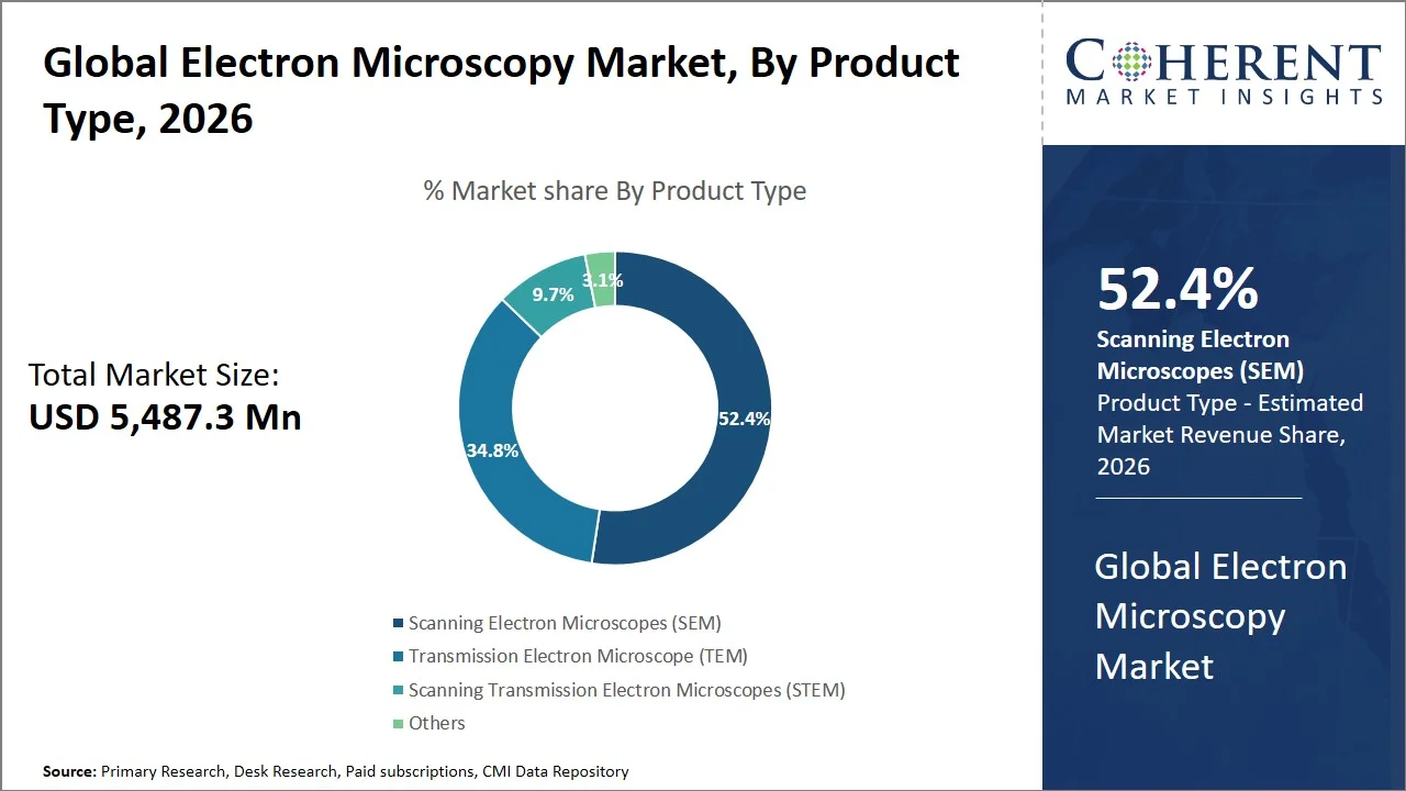
Why Do Scanning Electron Microscopes (SEM) Dominate the Global Electron Microscopy Market?
Scanning Electron Microscopes (SEM) are projected to hold a market share of 52.4% in 2026, owing to their flexibility in high-resolution imaging, analysis, and inspection of surfaces and defects in materials such as semiconductors, high-end products, and in quality control within numerous industries. The growing application in the characterization of various specimen without the need of pre-treatment and integration of automated imaging and analysis functionalities in these microscopes are some factors augmenting the adoption of SEMs. For instance, in April 2025, the National Institute of Standards and Technology (NIST) announced the release of a research paper, “High-Accuracy Interpretable Scanning Electron Microscope Image Analytics for the Semiconductor Industry,” designed to strengthen understanding of scanning electron microscope (SEM) images for semiconductor inspection and testing. The paper’s output further enables nanoscale defect analysis to be more accurate and expand the adoption of SEM in cutting-edge semiconductor applications and measurements.
- Current Industry Events of 2026
- Market Size Estimation
- Regional Breakdown
- Competitive Landscape
- Customer Intelligence
- Segmental Analysis
- Pricing Analysis
- Key Market Drivers, Challenges & Future Trends
- Customized Insights Section
Why Does the Material Sciences Segment Represent the Largest Application in the Electron Microscopy Market?
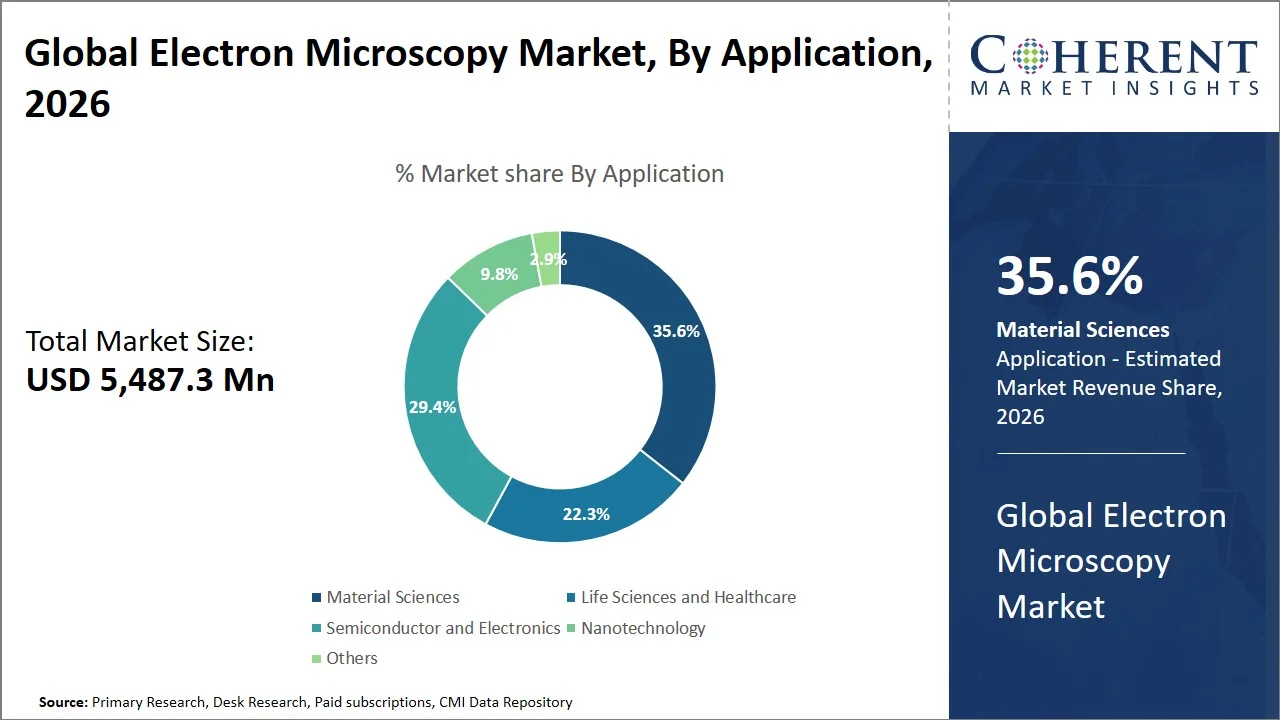
Material sciences are projected to hold a market share of 35.6% in 2026, due to its demand for nano characterization of the ceramics, composites, metals, battery components and polymer materials. Electron microscopy is key for detailing micro structures, crystal boundaries, defect and interface and is important in determining the effective structural parameters for creating high performance metals and alloys used for aerospace, aviation, and energy applications. In addition, the growing synergy between experimental microscopy and computational materials research facilitate greater adoption across academic and industrial laboratories. For instance, in October 2025, the U.S. Department of Energy (DOE) awarded USD 179 million in funding for 40 projects within the microelectronics science research centers that focus on advancing materials and semiconductors in which electron microscopy plays an indispensable role in analyzing at nanoscale and defect examination.
Academic and Research Institutes Segment Dominates the Global Electron Microscopy Market
The academic and research institutes segment is projected to hold a market share of 39.8% in 2026, due to consistent requirements for high resolution analysis for materials science, structural biology, nanotechnology, environmental sciences and research based in semiconductors. Academic and research institutes contribute significant share due to constant need for sophisticated instruments to explore science with high resolution and to gain in depth insight for innovation and training work force. They play central role in scientific discoveries and the validation of technologies. For instance, in June 2025, the European Research Council (ERC) granted USD 840 million (€721 million) to 281 frontier research projects as part of its Advanced Grant 2024 competition. Many of these grants are in the field of material science, nanotechnology and life science, boosting the funding into the next-generation of advanced research facilities, such as electron microscopy facilities.
Currents Events and their Impact
Current Events | Description and its Impact |
European Union Health Technology Assessment (HTA) Regulation Implementation (January 2025) |
|
U.S. FDA Strategic Roadmap for New Approach Methodologies (NAMs) (April 2025) |
|
Electron Microscopy Market Dynamics
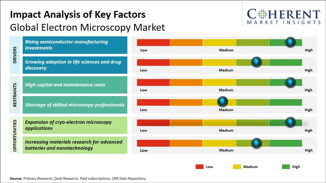
Market Drivers
- Rising semiconductor manufacturing investments: The rapid expansion of semiconductor manufacturing is driving the demand for electron microscopy systems used for nanoscale defect inspection, process optimization, and failure analysis. As chipmakers transition to advanced process nodes and heterogeneous packaging technologies, high-resolution imaging has become indispensable for maintaining production quality and yield. For instance, in April 2025, the U.S. Department of Commerce finalized a CHIPS Incentives Program award of up to USD 6.6 billion for Taiwan Semiconductor Manufacturing Company (TSMC) to expand advanced semiconductor manufacturing in Arizona. The investment is expected to strengthen demand for high-performance electron microscopy systems across wafer fabrication, metrology, and quality control applications.
- Growing adoption in life sciences and drug discovery: The widespread adoption of electron microscopy in life sciences and drug discovery is driving the demand for ultra-high-resolution imaging systems capable of visualizing cellular structures, proteins, viruses, and biomolecular interactions. Advancements in structural biology and precision medicine are encouraging pharmaceutical companies and research institutes to integrate electron microscopy into target identification, biologics development, and vaccine research. For instance, in September 2025, the U.S. National Institutes of Health (NIH) awarded new funding through its High-End Instrumentation (HEI) Grant Program to support the acquisition of state-of-the-art research instruments, including advanced electron microscopy systems, for biomedical research institutions. These investments are expected to strengthen the adoption of electron microscopy across drug discovery and translational research.
Emerging Trends
- Increasing Adoption of Cloud-Connected Electron Microscopy Platforms: Electron microscope manufacturers are increasingly integrating cloud-based data management and remote collaboration capabilities into their platforms. These solutions enable researchers to securely access, analyze, and share high-resolution imaging data across geographically dispersed teams, improving research efficiency and supporting multi-site collaborations.
- Growing Demand for Automated High-Throughput Electron Microscopy: Research laboratories and industrial users are increasingly adopting high-throughput, automated electron microscopy systems to accelerate sample analysis and improve reproducibility. Advances in robotic sample handling, AI-assisted image acquisition, and automated defect detection are reducing operator intervention while significantly increasing laboratory productivity, particularly in semiconductor inspection and materials characterization.
Regional Insights
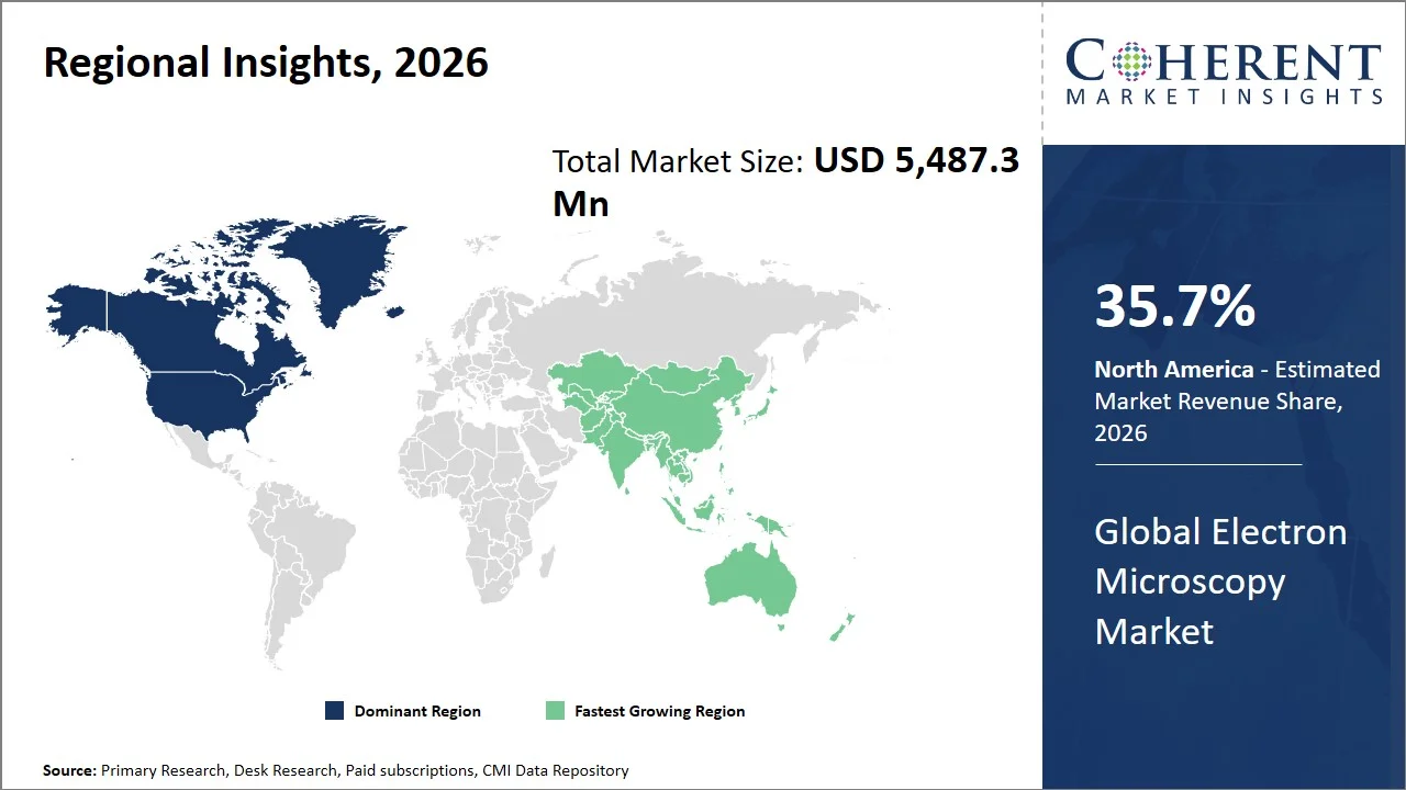
Why is North America a Strong Market for Electron Microscopy?
North America leads the global electron microscopy market, accounting for an estimated 35.7% share in 2026, due to its matured ecosystem of nanotechnology, biotechnology, material science, and semiconductors that maintain steady adoption of advanced high resolution analytical instruments. Abundant government support for scientific exploration, high penetration of advanced characterization techniques, and increasing collaboration between federal labs, universities and industry research centers facilitate the deployment of electron microscopy systems across life sciences, advanced materials and nanotechnologies application. For instance, the U.S. National Nanotechnology Initiative (NNI) requested a historic USD 2.2 billion in FY2025 for nanoscale science and engineering research in 12 federal agencies. The increased investment will expand nanoscale infrastructure to broaden the implementation of sophisticated electron microscopy systems for both characterization of nanomaterials and a broad array of interdisciplinary science.
Why Does the Asia Pacific Electron Microscopy Market Exhibit High Growth?
The Asia Pacific electron microscopy market is expected to exhibit the fastest growth with an estimated contribution of 29.6% share to the global market in 2026, due to rapid increase in the budget of scientific research as well as growing the expenditure for electronic manufacturing industry, drug industry, and automotive sector materials industries owing to extensive use of the electron microscopes in quality control, product development, and analysis. The speedy expansion of high-resolution electron microscopes on advance manufacturing and public research infrastructures is likely to push the market for the adoption of these analytical techniques. For instance, in FY2025, Japan boosted its science and technology related budget to an all-time high of USD 31.1 billion (JPY5.05 trillion), as part of its 6th Science, technology and innovation basic plan. High-level research infrastructure development projects in nanotechnology, material science and life sciences will likely create new demand for high-end instruments such as electron microscopy systems. (Source: Japan Science and Technology Agency)
Global Electron Microscopy Market Outlook for Key Countries
Why is the U.S. Leading Innovation and Adoption in the Electron Microscopy Market?
The U.S. dominates the electron microscopy market driven by an advanced infrastructure that leverages electron microscopy for structural biology, translational medical research, materials science, and in semiconductor process development. With a rich history of technology and a well-developed framework of microscope manufacturers (such as Thermo Fisher Scientific, Bruker Corporation), end-users (such as Harvard University, Mayo Clinic) and contract research facilities (such as Charles River Laboratories, Labcorp Drug Development), the U.S. offers ground for early commercialization of next-generation microscopy. Increasing need for multimodal capabilities and AI automation in microscopy workflows will accelerate uptake of electron microscopy within the country.
Is Japan a Favorable Market for Electron Microscopy Market?
Japan is one of the most promising markets for the electron microscopy market, due to its high penetration in the areas of semiconductor production, new material technologies and precision engineering. Japan employs electron microscopes for wafer inspections, characterization of new material, battery research and manufacturing quality control. The well-established innovative infrastructure of Japan, and their focus on high resolution, detailed analysis technology contributes to the robust demand for sophisticated electron microscope systems.
Is China Emerging as a Key Growth Hub for the Electron Microscopy Market?
China is positioned as a key growth hub in the global electron microscopy market due to expansion in semiconductor fabrication, nanotechnology research and development, modern equipment manufacturing and battery material development. Growing domestic need for sophisticated resolution imaging devices and capabilities used in electronics, life science and manufacturing industries drive the demand growth of electron microscopy in the country. Further, rising investments in infrastructure development for science, development of indigenous technologies makes it one of the rapidly growing electron microscopy market globally.
Why Does Germany Top the European Electron Microscopy Market?
Germany leads the Europe electron microscopy market owing to its sophisticated and well-developed base for high-tech manufacturing, automotive technology, materials science, and industrial research and development. In Germany, the usage of electron microscopy is particularly high in metallurgical studies, the inspection of semiconductors and batteries, and for materials research in the field of precision engineering. Furthermore, the existence of a deep-rooted network of industrial laboratories (such as Fraunhofer Institutes, TÜV Rheinland), research institutes (such as Max Planck Society, Helmholtz Association), and high-tech manufacturing industries (such as Infineon Technologies, Bosch) ensures a continuing market need for high-end electron microscopes.
Is the Electron Microscopy Market Developing in South Korea?
South Korea is a high-potential market for electron microscopy due to its world-class leadership in chip production, screen manufacturing and high-performance batteries. The country leverages electron microscopy in wafer inspections, failure analysis, and in researching the materials used for the production of high-performance batteries. An active ecosystem, consisting of a number of chip manufacturers (such as Samsung Electronics, SK Hynix), research centers (such as Korea Advanced Institute of Science and Technology (KAIST), Korea Institute of Science and Technology (KIST)), and corporate research & development facilities, drive even higher levels of innovation in electron microscopy systems for the next generation of applications.
Product Innovation Landscape in the Global Electron Microscopy Market
Company | Product / Platform | Key Innovation | Target Application | Market Significance |
Thermo Fisher Scientific Inc. | Scios 3 FIB-SEM & Talos 12 TEM | AI-enabled automation, simplified workflows, enhanced imaging performance | Life sciences, semiconductor inspection, materials research | Improves laboratory productivity and broadens accessibility to advanced electron microscopy. |
Hitachi High-Tech Corporation | SU9600 SEM | Ultrahigh-resolution imaging, automated data acquisition, Cold Field Emission (CFE) electron gun | Semiconductor manufacturing, nanotechnology, advanced materials | Enables high-throughput nanoscale characterization and defect analysis for next-generation semiconductor devices. |
Carl Zeiss AG | ZEN core for SEM | Unified software platform with integrated imaging, analytics, and EDS workflows | Industrial QA/QC, life sciences, materials science | Enhances workflow efficiency through connected microscopy and centralized instrument control. |
Shimadzu Corporation | SUPERSCAN SS-3000 / SS-4000 Series (Shimadzu by TESCAN) | Low-vacuum SEM operation, automated beam alignment, simplified operation | Materials characterization, industrial R&D, quality control | Expands access to high-performance SEM solutions while improving ease of use for routine analytical applications. |
JEOL Ltd. | JEM-120i TEM | Compact design, automated alignment, intuitive user interface | Academic research, life sciences, pathology | Simplifies TEM operation, enabling faster adoption by research laboratories and educational institutions. |
TESCAN GROUP, a.s. | CLARA SEM Platform | High-resolution field-emission imaging with advanced analytical integration | Semiconductor inspection, metallurgy, nanomaterials | Strengthens precision materials characterization and supports advanced industrial research workflows. |
How is the expansion of cryo-electron microscopy applications creating new growth opportunities in the electron microscopy market?
Increased adoption of Cryo-EM technology in structural biology, biologic manufacturing, and personalized medicine sector, driven by need of determining protein structure, antibodies and develop new medicines, presents major expansion opportunities for the electron microscopy market. Its ability to visualize biomolecules at near-atomic resolution is accelerating protein structure determination, antibody discovery, and drug development. For instance, in April 2025, Thermo Fisher Scientific Inc. unveiled Krios 5 Cryo-Transmission Electron Microscope (Cryo-TEM) with advanced optics, increased throughput by up to 25%, and a set of AI-driven features for the higher resolution structural biology and drug development research.
Market Players, Key Development, and Competitive Landscape
Key Developments
- In December 2025, Shimadzu Corporation announced its agreement to acquire TESCAN GROUP, a Czech-based manufacturer of scanning electron microscopes (SEMs) and focused ion beam (FIB) systems, for approximately USD 678 million. The acquisition is aimed at strengthening Shimadzu's presence in advanced analytical instrumentation and expanding its electron microscopy portfolio. The transaction is expected to enhance the company's technological capabilities and global competitiveness in materials science, semiconductor, and life sciences research.
- In October 2025, Hitachi High-Tech Corporation launched the SU9600, a next-generation ultrahigh-resolution scanning electron microscope (SEM) that combines sub-nanometer imaging with enhanced automation and high-throughput data acquisition. The system is designed to support advanced semiconductor inspection, materials characterization, and nanotechnology research while addressing the growing need for AI-driven large-scale data analysis. The launch strengthens the company's electron microscopy portfolio and is expected to accelerate the adoption of high-performance analytical instruments across research and industrial applications.
- In July 2025, Thermo Fisher Scientific Inc. launched the Scios 3 DualBeam FIB-SEM and Talos 12 Transmission Electron Microscope at the Microscopy & Microanalysis (M&M) 2025 Conference. The new electron microscopy platforms incorporate enhanced automation, improved imaging performance, and streamlined workflows to increase laboratory productivity across life sciences, semiconductor research, and advanced materials characterization. The launch further strengthens Thermo Fisher's portfolio of high-performance analytical instruments and supports the growing demand for next-generation electron microscopy solutions.
Competitive Landscape
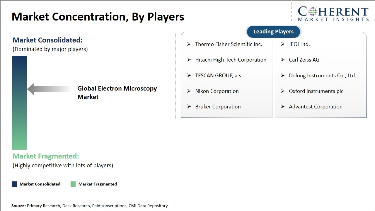
The global electron microscopy market is moderately consolidated, with competition centered on technological innovation, imaging precision, workflow automation, and application-specific capabilities across life sciences, semiconductors, materials science, and nanotechnology. Market participants are investing in next-generation electron optics, AI-powered image analysis, and integrated analytical software to improve imaging performance, throughput, and user accessibility. Strategic collaborations with research institutions, expansion of manufacturing and service networks, and continuous product innovation remain key competitive strategies as demand for high-resolution characterization technologies continues to grow. Key focus areas include:
- Development of AI-enabled, high-throughput electron microscopy platforms
- Expansion of cryo-electron microscopy and multimodal imaging portfolios
- Integration of advanced analytical software and automated image analysis
- Strengthening presence in semiconductor, life sciences, and advanced materials research
- Strategic acquisitions, research collaborations, and global service network expansion
Market Report Scope
Electron Microscopy Market Report Coverage
| Report Coverage | Details | ||
|---|---|---|---|
| Base Year: | 2025 | Market Size in 2026: | USD 5,487.3 Mn |
| Historical Data for: | 2020 To 2024 | Forecast Period: | 2026 To 2033 |
| Forecast Period 2026 to 2033 CAGR: | 7.3% | 2033 Value Projection: | USD 8,964.8 Mn |
| Geographies covered: |
| ||
| Segments covered: |
| ||
| Companies covered: | Thermo Fisher Scientific Inc., JEOL Ltd., Hitachi High-Tech Corporation, Carl Zeiss AG, TESCAN GROUP, a.s., Delong Instruments Co., Ltd., Nikon Corporation, Oxford Instruments plc, Bruker Corporation, and Advantest Corporation | ||
| Growth Drivers: |
| ||
| Restraints & Challenges: |
| ||
Analyst Opinion (Expert Opinion)
- In the coming years, the global electron microscopy market will be shaped by continued advancements in AI-assisted imaging, automation, cryo-electron microscopy (Cryo-EM), and high-resolution analytical capabilities, with demand expanding beyond academic research into semiconductor manufacturing, advanced materials, and precision medicine. As industries increasingly require nanoscale characterization and real-time materials analysis, electron microscopy will become an indispensable tool across both research and industrial environments.
- The maximum opportunities will probably exist within Scanning Electron Microscopes (SEM) for semiconductor inspection and failure analysis in Asia Pacific, particularly in China, South Korea, Taiwan, and Japan, where substantial investments in advanced chip manufacturing, packaging technologies, and government-supported semiconductor programs continue to accelerate demand for high-performance electron microscopy systems.
- In order to obtain a competitive advantage, market participants should focus on developing AI-enabled and automated imaging platforms, expanding application-specific solutions for semiconductors and life sciences, and strengthening digital software ecosystems through cloud connectivity and advanced image analytics. Enhancing global service capabilities, user training, and collaborative partnerships with research institutes and industrial customers will further differentiate vendors in an increasingly technology-driven market.
Speak to the analyst
Want personalized insights?
Take the findings above to one of our principal consultants, or have the report rebuilt around the segments, geographies and competitors you actually track.
Market Segmentation
- Product Type Insights (Revenue, USD Mn, 2021 - 2033)
- Scanning Electron Microscopes (SEM)
- Transmission Electron Microscope (TEM)
- Scanning Transmission Electron Microscopes (STEM)
- Others
- Application Insights (Revenue, USD Mn, 2021 - 2033)
- Material Sciences
- Life Sciences and Healthcare
- Semiconductor and Electronics
- Nanotechnology
- Others
- End User Insights (Revenue, USD Mn, 2021 - 2033)
- Academic and Research Institutes
- Pharmaceutical and Biotechnology Companies
- Semiconductor and Electronics Companies
- Industrial and Manufacturing Companies
- Contract Research Organizations (CROs)
- Others
- Regional Insights (Revenue, USD Mn, 2021 - 2033)
- North America
- U.S.
- Canada
- Latin America
- Brazil
- Argentina
- Mexico
- Rest of Latin America
- Europe
- Germany
- U.K.
- Spain
- France
- Italy
- Russia
- Rest of Europe
- Asia Pacific
- China
- India
- Japan
- Australia
- South Korea
- ASEAN
- Rest of Asia Pacific
- Middle East
- GCC Countries
- Israel
- Rest of Middle East
- Africa
- South Africa
- North Africa
- Central Africa
- North America
- Key Players Insights
- Thermo Fisher Scientific Inc.
- JEOL Ltd.
- Hitachi High-Tech Corporation
- Carl Zeiss AG
- TESCAN GROUP, a.s.
- Delong Instruments Co., Ltd.
- Nikon Corporation
- Oxford Instruments plc
- Bruker Corporation
- Advantest Corporation
Sources
Primary Research Interviews
- Electron Microscope Manufacturers
- Material Science Researchers & Scientists
- Semiconductor & Nanotechnology Industry Experts
- Healthcare & Life Sciences Laboratory Professionals
- Others
Stakeholders
- Electron microscopy instrument manufacturers
- Electron detector, imaging software, and analytical solution providers
- Contract Research Organizations (CROs) and Contract Development & Manufacturing Organizations (CDMOs)
- Semiconductor fabrication companies and electronics manufacturers
- Academic and government-funded research laboratories
- End-use Sectors
- Academic and Research Institutes
- Pharmaceutical and Biotechnology Companies
- Semiconductor and Electronics Industry
- Materials Science and Nanotechnology Laboratories
- Industrial Manufacturing and Quality Control Laboratories
- Regulatory & Health Bodies
- U.S. Food and Drug Administration (FDA)
- National Institutes of Health (NIH), U.S.
- National Science Foundation (NSF), U.S.
- European Commission – Horizon Europe
- Ministry of Economy, Trade and Industry (METI), Japan
- Ministry of Trade, Industry and Energy (MOTIE), South Korea
Databases
- NIH RePORTER Database
- ClinicalTrials.gov
- NSF Awards Database
- CORDIS (EU Research Projects Database)
- OECD Main Science and Technology Indicators (MSTI)
- UNESCO Institute for Statistics (UIS)
Magazines
- Microscopy Today
- Advanced Materials Magazine
- Scientific American
- Nature Photonics
Journals
- Journal of Microscopy (Wiley)
- Ultramicroscopy (Elsevier)
- Journal of Electron Microscopy
Associations
- Microscopy Society of America (MSA)
- Royal Microscopical Society (RMS)
- European Microscopy Society (EMS)
- International Federation of Societies for Microscopy (IFSM)
Public Domain Sources
- U.S. Food and Drug Administration (FDA)
- National Institutes of Health (NIH)
- European Commission – Research & Innovation
- U.S. Department of Energy (DOE)
Proprietary Elements
- CMI Data Analytics Tool, Proprietary CMI Existing Repository of information for last 10 years.
Get access to 250+ pages report
Every segment, forecast, competitor profile and data table behind the analysis above — available for instant download.
- ESOMAR Member
- ISO 9001:2015 Certified
- D-U-N-S Registered
- GDPR & CCPA Compliant
Missing comfort of reading report in your local language? Find your preferred language:
Transform your Strategy with Exclusive Trending Reports
Frequently Asked Questions
The global electron microscopy market is estimated to be valued at USD 5,487.3 Mn in 2026 and is expected to reach USD 8,964.8 Mn by 2033.
Scanning Electron Microscopes (SEM) dominate due to their versatility, high-resolution surface imaging capabilities, relatively lower operating costs compared to TEM, and widespread use in semiconductor inspection, materials science, industrial quality control, and nanotechnology research.
Electron microscopy is an advanced imaging technique that uses a focused beam of electrons to generate ultra-high-resolution images of materials and biological specimens at the nanometer and atomic scale.
The CAGR of the global electron microscopy market is projected to be 7.3% from 2026 to 2033.
In terms of end user, academic and research institutes are estimated to dominate the market revenue share in 2026.
Scanning Electron Microscopes (SEM) generate high-resolution three-dimensional surface images, whereas Transmission Electron Microscopes (TEM) transmit electrons through thin specimens to reveal internal structures at near-atomic resolution.
Electron microscopy is widely used for semiconductor failure analysis, materials characterization, nanotechnology research, structural biology, drug discovery, and industrial quality control.