

Extreme Ultraviolet (EUV) Lithography Market Analysis & Forecast
Global Extreme Ultraviolet (EUV) Lithography Market is estimated to be valued at USD 20,568.2 Mn in 2026 and is expected to reach USD 153,013.7 Mn by 2033, exhibiting a compound annual growth rate (CAGR) of 33.2% from 2026 to 2033.
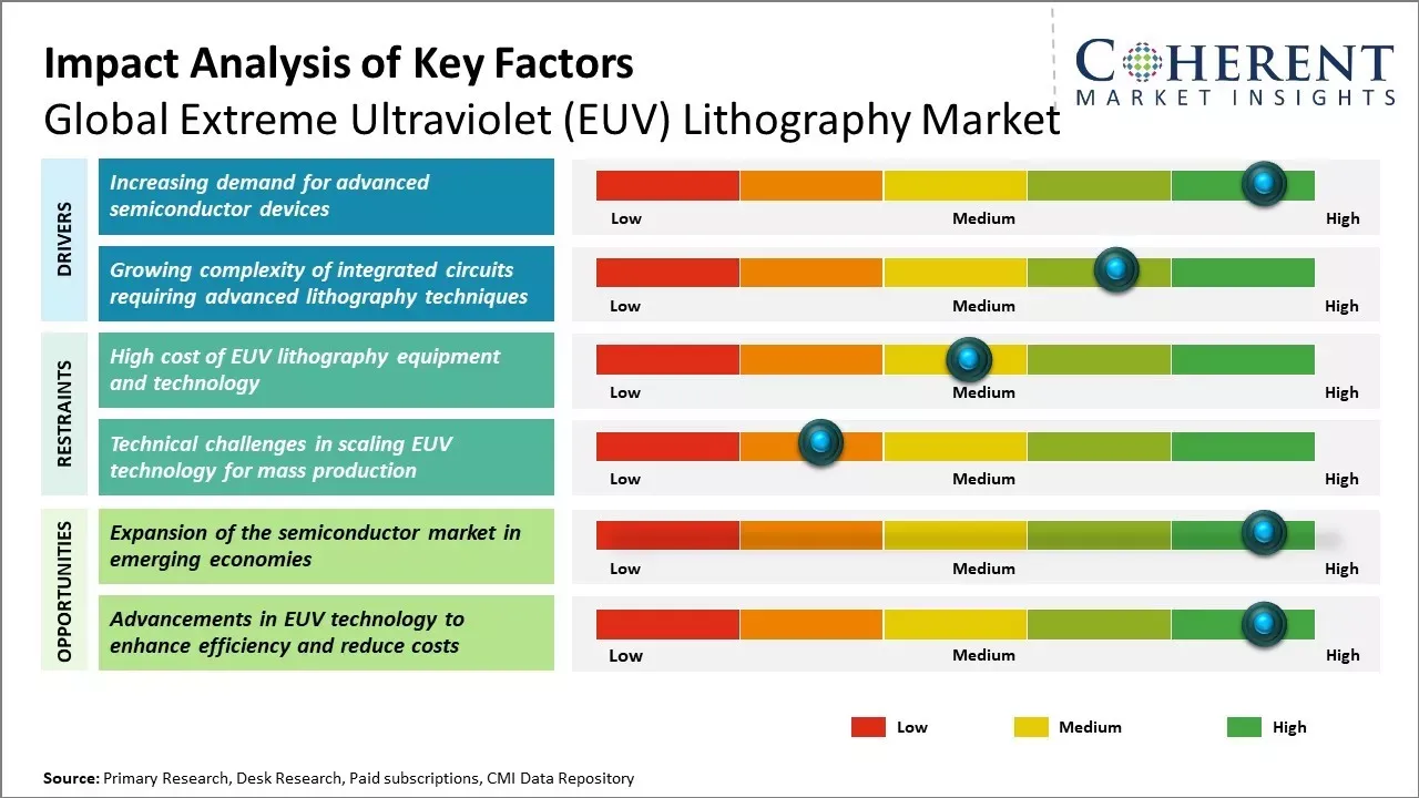
Key Takeaways
- Based on Equipment, the light source segment is projected to dominate the global EUV lithography market with a 35.1% share in 2026, as they are the core component enabling precise patterning at advanced nodes like 3 nm and 2 nm.
- By End User, the Foundry segment is expected to hold the highest share in 2026 within the global EUV lithography market, due to its focus on advanced-node semiconductor manufacturing
- By Region, Aisa Pacific is estimated to lead the market with a share of 40.2% in 2026. While, North America, holding an estimated share of 26.8% in 2026, is projected to be the fastest growing region.
Market Overview
The global Extreme Ultraviolet (EUV) Lithography Market demand is experiencing strong growth, propelled by rising demand for advanced semiconductor manufacturing and miniaturized chip designs. The need for higher-resolution patterning has accelerated the adoption of EUV technology, enabling production at sub-7nm nodes. Lithography equipment dominates the market, with semiconductor manufacturing as the key application segment.
Current Events and its Impact on the Extreme Ultraviolet (EUV) Lithography Market
Current Event | Description and its impact |
Technological Advancements in Semiconductor Fabrication |
|
Surging Demand for AI and High-Performance Computing (HPC) |
|
Geopolitical Tensions and Export Controls |
|
Role of Artificial Intelligence in Extreme Ultraviolet (EUV) Lithography Market
Artificial Intelligence plays a transformative role in analyzing extreme ultraviolet (EUV) imagery, particularly for space weather forecasting. By processing vast amounts of high-resolution EUV data from solar observatories, AI can detect subtle, early signs of solar flares and other solar activities that are invisible to traditional methods.
In August 2025, IBM and NASA unveiled Surya, an AI model that predicts solar flares up to two hours in advance with 16% more accuracy and half the response time of existing tools. Trained on nine years of solar data, it comes as solar activity nears its peak, helping protect satellites, power grids, and communications from potentially catastrophic flares.
- Current Industry Events of 2026
- Market Size Estimation
- Regional Breakdown
- Competitive Landscape
- Customer Intelligence
- Segmental Analysis
- Pricing Analysis
- Key Market Drivers, Challenges & Future Trends
- Customized Insights Section
Segmental Insights
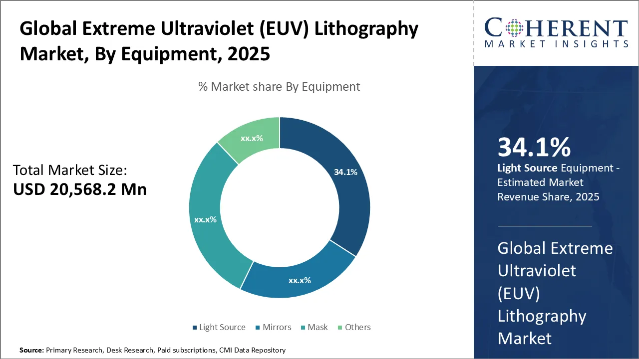
Extreme Ultraviolet (EUV) Lithography Market Insights, By Equipment: Light Sources Leads the market as They Are the Core Component Enabling Precise Patterning
In terms of equipment, the light sources segment is projected to hold 35.1% share in 2026, as they are the core component enabling precise patterning at advanced nodes like 3 nm and 2 nm. High-intensity, stable light is essential for wafer throughput and production efficiency. Limited suppliers, technological complexity, and the global expansion of advanced semiconductor fabs further drive their dominance and rapid growth among EUV equipment components.
For instance, in August 2024, Japanese scientists at the Okinawa Institute of Science and Technology (OIST) developed a more energy-efficient and cost-effective extreme ultraviolet (EUV) lithography technology. Their approach utilizes compact EUV light sources, consuming less than one-tenth the power of conventional systems. This innovation reduces the number of mirrors from six to two, enhancing light efficiency and system stability.
-lithography-market-by-end-user.webp "Extreme Ultraviolet (EUV) Lithography Market, By End User")
Extreme Ultraviolet (EUV) Lithography Market Insights, By End User: Foundry is Demanding Due To Its Focus on Advanced-Node Semiconductor Manufacturing
In terms of end user, the foundry segment is expected to contribute the largest share of the market in 2026, due to its focus on advanced-node semiconductor manufacturing. Leading foundries like TSMC and Samsung produce high-performance chips at 5nm and below, which require EUV for fine patterning. Unlike IDMs, foundries prioritize cutting-edge nodes and high-volume, multi-client production, benefiting from improved yield and faster timelines. Strong capital investment and government support in regions like Taiwan and South Korea enable deployment of costly EUV machines. Additionally, growing client demand for advanced chips drives foundries to adopt EUV, solidifying their market dominance.
For instance, in April 2024, Intel Foundry has achieved a significant milestone by installing the industry's first commercial High Numerical Aperture (High NA) Extreme Ultraviolet (EUV) lithography system at its Fab D1X in Hillsboro, Oregon. Developed in collaboration with ASML, the 165-ton TWINSCAN EXE:5000 tool is poised to enhance chip manufacturing precision, enabling the production of smaller transistors and more powerful processors.
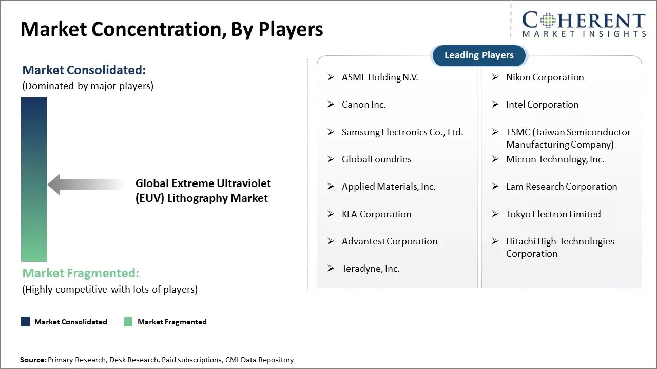
Market Concentration and Competitive Landscape
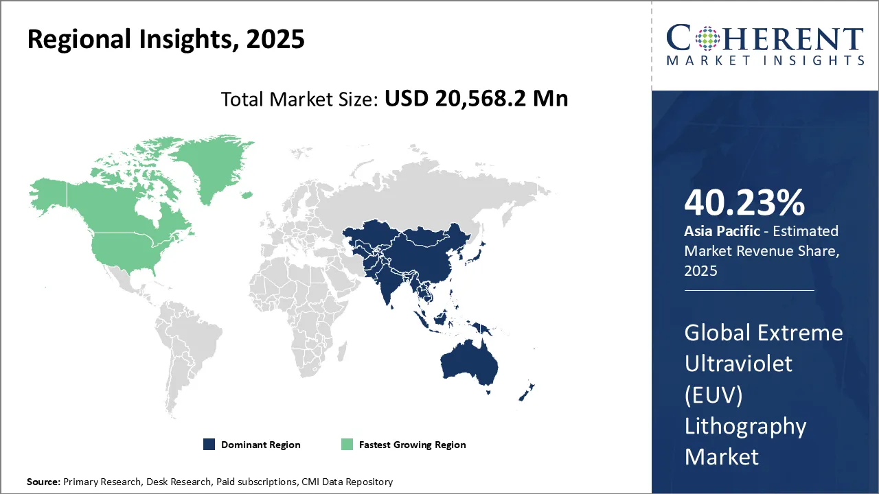
Extreme Ultraviolet (EUV) Lithography Market: Regional Insights
Asia Pacific Extreme Ultraviolet (EUV) Lithography Market Analysis and Trends
The Asia Pacific region is projected to lead the market with a 40.2% share in 2026. The region hosts major semiconductor foundries like TSMC, Samsung, and SMIC, producing advanced nodes that rely on EUV lithography. Strong government support and strategic investments in domestic semiconductor capabilities further boost demand. Additionally, Asia-Pacific’s leadership in consumer electronics, AI, automotive, and IoT drives the need for smaller, faster, and more efficient chips. Expansion of fabrication facilities and a robust supply chain make it easier to scale EUV technology, making the region both the largest and fastest-growing EUV market in 2026.
For instance, in October 2024, Fujifilm launched new negative-tone resists and developers for extreme ultraviolet (EUV) lithography, advancing semiconductor miniaturization. These materials, compatible with the evolved Negative Tone Imaging (NTI) process, enhance circuit pattern formation precision, addressing challenges like resist swelling during development. To support this innovation, Fujifilm is upgrading production and quality evaluation facilities in Shizuoka, Japan, and Pyeongtaek, South Korea.
North America Extreme Ultraviolet (EUV) Lithography Market Analysis and Trends
North America, holding an estimated share of 26.8% in 2026, exhibit the fastest growth in the global extreme ultraviolet (EUV) lithography market, due to several strategic and technological factors. Leading semiconductor companies like Intel, IBM, and Micron rely on EUV systems to produce advanced nodes, including 5nm and below, for high-performance computing, AI, and cloud applications. Government initiatives such as the CHIPS and Science Act provide funding and incentives, encouraging domestic investments in cutting-edge fabrication technologies. The region’s strong R&D ecosystem and growing demand for high-performance and specialty chips in aerospace, defense, automotive, and AI further drive EUV adoption. Additionally, supply chain security and technological independence motivate companies to strengthen domestic semiconductor capabilities, making North America a key market for EUV lithography.
For instance, in July 2026, Governor Kathy Hochul announced the grand opening of the CHIPS for America Extreme Ultraviolet (EUV) Accelerator at the NY CREATES Albany NanoTech Complex. The EUV Accelerator, operational is one of three National Semiconductor Technology Center (NSTC) flagship research and development facilities across the U.S. This state-of-the-art facility enables researchers from Natcast, NSTC member organizations, and NY CREATES to collaborate on advancing semiconductor technologies essential for national and economic security. The project is supported by significant private investment from industry leaders such as IBM, Micron, Applied Materials, and Tokyo Electron.
Extreme Ultraviolet (EUV) Lithography Market Outlook Country-Wise
The U.S. Extreme Ultraviolet (EUV) Lithography Market Trends
The United States holds the largest share of the EUV lithography market at 21%, reflecting its position as a global semiconductor leader. Major U.S. companies, such as Intel, Micron, and GlobalFoundries, are investing heavily in advanced chip manufacturing. Government initiatives like the CHIPS and Science Act further incentivize domestic semiconductor production, directly driving demand for EUV technology. Additionally, the U.S. focuses on high-performance computing, AI, and defense electronics, which require the precision and scalability that EUV lithography provides.
For instance, in February 2026, DuPont showcased advancements in extreme ultraviolet (EUV) lithography at the 2026 SPIE Advanced Lithography + Patterning Conference in San Jose, California. The company presented multiple technical sessions focused on enhancing resolution, line edge roughness, and sensitivity in EUV photoresists. These presentations will highlight developments from DuPont's new EON™ EUV photoresist platform and novel compositions for next-generation EUV lithography.
The U.K. Extreme Ultraviolet (EUV) Lithography Market Trends
The United Kingdom accounts for approximately 6% of the EUV lithography market. The demand here is relatively moderate because the U.K. has a limited semiconductor manufacturing base. Most EUV usage is concentrated in R&D labs and design centers for prototyping and research purposes. However, growing investments in AI, quantum computing, and semiconductor research are gradually increasing the country’s engagement with EUV technology.
For instance, in April 2026, the University of Southampton inaugurated Europe's first electron beam (E-beam) lithography facility, a pioneering step in semiconductor chip development. This state-of-the-art facility, the second globally and the first outside Japan, employs electron beams to etch ultra-precise patterns onto chips, enabling advancements in AI, medical diagnostics, and defense technologies. The UK government has also announced a £4.75 million investment to enhance the semiconductor talent pipeline, funding bursaries, chip design courses, and school outreach programs.
China Extreme Ultraviolet (EUV) Lithography Market Trends
China represents 15% of the global EUV lithography market, driven by its aggressive push to develop a self-reliant semiconductor industry. Through initiatives like Made in China 2026, the country is investing heavily in foundries capable of producing advanced nodes, such as 7nm and 5nm chips, which require EUV lithography. Government support, coupled with a growing demand for electronics and AI applications, makes China one of the fastest-growing markets for EUV technology.
For instance, in February 2026, China announced a €37 billion initiative to develop domestic extreme ultraviolet (EUV) lithography systems, aiming to reduce reliance on Western semiconductor technology. Currently, ASML, a Dutch company, holds a near-monopoly on EUV machines, essential for producing advanced semiconductor nodes at 5 nm and below. The EUV process involves generating 13.5 nm wavelength light by targeting tin droplets with high-power lasers, creating a plasma that emits the required radiation.
Brazil Extreme Ultraviolet (EUV) Lithography Market Trends
Brazil contributes around 3% to the global EUV lithography market, reflecting its relatively small semiconductor ecosystem. Most of the demand is associated with research institutions or niche electronics applications, rather than large-scale semiconductor production. Consequently, EUV adoption in Brazil remains limited, focused primarily on academic and experimental purposes.
For instance, in September 2024, Brazil has announced a BRL 186.6 billion investment to modernize its industrial sector through digital transformation. The initiative, known as Mission 4 of the New Industry Brazil (NIB), aims to integrate the country into global high-tech supply chains, enhancing competitiveness and creating skilled jobs. The government has also approved the Brazil Semicon Act, providing BRL 7 billion in annual incentives for the semiconductor and Information and Communications Technology sectors.
GCC Countries Extreme Ultraviolet (EUV) Lithography Market Trends
The GCC countries, including the UAE and Saudi Arabia, account for 3% of the EUV lithography market. While there are investments in technology and electronics infrastructure, domestic semiconductor manufacturing is minimal. The demand for EUV lithography is mainly in research centers and emerging tech initiatives, with limited large-scale production. Efforts are ongoing to develop a stronger regional semiconductor ecosystem, which may increase EUV adoption in the future.
For instance, Egypt, Saudi Arabia, and Oman are advancing the Middle East's semiconductor industry through distinct strategies. Egypt is leveraging its established engineering talent and the "Egypt Makes Electronics" initiative to foster a robust fabless ecosystem. Saudi Arabia is investing heavily, launching the National Semiconductor Hub with a $266 million fund to attract 50 design companies by 2030. Oman is taking a collaborative approach, focusing on outsourced semiconductor assembly and testing (OSAT) and establishing an IC design center with GSME.
Market Report Scope
Extreme Ultraviolet (EUV) Lithography Market Report Coverage
| Report Coverage | Details | ||
|---|---|---|---|
| Base Year: | 2025 | Market Size in 2026: | USD 20,568.2 Mn |
| Historical Data for: | 2020 To 2024 | Forecast Period: | 2026 To 2033 |
| Forecast Period 2026 to 2033 CAGR: | 33.2% | 2033 Value Projection: | USD 153,013.7 Mn |
| Geographies covered: |
| ||
| Segments covered: |
| ||
| Companies covered: | Canon Inc., Samsung Electronics Co. Ltd, Toppan Photomasks Inc., Ushio, Inc., ASML Holding NV, NTT Advanced Technology Corporation, Nikon Corporation | ||
| Growth Drivers: |
| ||
| Restraints & Challenges: |
| ||
Market Dynamics
Extreme ultraviolet (EUV) lithography market Trends
Increasing Demand for Advanced Semiconductor Devices
Rising demand for more powerful smartphones, computers, and electronic devices is driving the Extreme Ultraviolet (EUV) lithography market demand. Advanced devices require faster processors, higher memory, and support for AI, machine learning, and 5G, increasing data processing needs. Semiconductor manufacturers face pressure to miniaturize components and integrate more transistors per chip, necessitating advanced lithography. With conventional optical lithography nearing its limits, EUV lithography enables finer lines and spaces below the 7nm node, supporting next-generation logic and memory chip development.
Growing Complexity of Integrated Circuits Requiring Advanced Lithography Techniques
The relentless drive to integrate more transistors on the same silicon to enhance functionality, efficiency, and affordability has intensified challenges in device miniaturization. Emerging technologies like AI, IoT, and autonomous vehicles demand higher performance at lower power, pushing chipmakers to integrate billions of transistors on a single die—a feat beyond the capabilities of traditional lithography tools. Multi-patterning techniques, while useful, are costly and reduce productivity. Extreme ultraviolet (EUV) lithography market share is growing as EUV enables precise printing of tiny features in a single exposure, overcoming density bottlenecks. Leading foundries are collaborating with vendors to accelerate EUV adoption, supporting next-generation high-density, high-performance chips.
For instance, in January 2024, ZEISS Group, a leading provider of optical systems and semiconductor manufacturing technology, unveiled its High-NA (Numerical Aperture) Extreme Ultraviolet (EUV) lithography system. This advanced system marks a significant advancement in semiconductor manufacturing, enabling the production of microchips with exceptionally fine features, surpassing the capabilities of existing EUV systems. The High-NA-EUV technology will facilitate the creation of more powerful, energy-efficient, and cost-effective chips, setting the stage for the next generation of integrated circuits.
Extreme Ultraviolet (EUV) Lithography Market Opportunities
Expansion of Semiconductor Market in Emerging Economies
The Extreme Ultraviolet (EUV) lithography market forecast indicates strong growth potential driven by the expansion of the overall semiconductor market in emerging economies. Countries such as China, India, Brazil, Indonesia, and others are experiencing rapid economic development, which fuels the growth of multiple industries and increases the demand for electronic products. This trend has a direct positive impact on the semiconductor sectors in these nations.
Additionally, the market for devices like smartphones and computers is witnessing exponential growth in the developing world. This rising need for sophisticated semiconductors creates significant opportunities for EUV lithography technology to be adopted on a wider scale within the semiconductor industries of emerging economies in the coming years.
Analyst Opinion (Expert Opinion)
The Extreme Ultraviolet (EUV) Lithography Market is at a critical inflection point, driven by the demand for advanced semiconductor manufacturing in AI, data centers, and automotive electronics. TSMC’s commitment to 2nm chips by 2025 exemplifies the industry's push toward smaller nodes.
ASML, the sole EUV machine supplier, continues to innovate with high-NA systems, evidenced by €7.1 billion in net bookings, highlighting robust demand from AI chip producers. Policy developments, such as the U.S.-EU tariff exemption for semiconductor equipment, further support cost efficiencies for global manufacturers.
Challenges persist: EUV machines cost ~$400 million, creating high capital expenditure pressures. Alternative techniques like nanoimprint lithography and reliance on a limited supplier base for critical components pose additional constraints.
Overall, the market’s growth is promising, but stakeholders must balance the Extreme Ultraviolet (EUV) Lithography Market Value and Price against technological complexity and financial risk to ensure sustainable adoption.
Speak to the analyst
Want personalized insights?
Take the findings above to one of our principal consultants, or have the report rebuilt around the segments, geographies and competitors you actually track.
Extreme Ultraviolet (EUV) Lithography Market: Key Development
- In June 2025, ASML announced the shipment of its third High-NA EUV lithography system, with an order backlog of 10–20 units from key clients like Intel, TSMC, Samsung, and Micron. Each tool is valued at approximately €350 million. The scaling of High-NA EUV tool production indicates a strong market shift toward next-generation chip manufacturing. However, high costs may limit accessibility to only the top-tier fabs, concentrating adoption among industry giants.
- In January 2025, Chinese researchers reported significant progress on a homegrown EUV scanner using laser-induced plasma, targeting pilot production in Q3 2025 and volume manufacturing in 2026. If realized, this would break ASML’s monopoly, reshaping global competition and potentially mitigating geopolitical pressure on EUV tool access in Asia.
- In June 2024, ASML and Belgium’s imec inaugurated the world’s first High-NA EUV research lab in Veldhoven. The site houses the TWINSCAN EXE:5000 and enables early process development for future 2nm and below nodes. The lab accelerates ecosystem readiness for High-NA EUV, giving chipmakers access to early testing and speeding up commercial rollout.
- In December 2024, ASML shipped its first High-NA EUV lithography system (EXE:5000) to Intel’s Oregon R&D site for sub-2nm process development. Intel’s early adoption places it at the forefront of lithography innovation. This milestone also marks the start of commercial High-NA EUV deployment in the global semiconductor industry.
Market Segmentation
- Equipment Insights (Revenue, USD Mn, 2026 - 2033)
- Mask
- Mirrors
- Light Sources
- Others
- End User Insights (Revenue, USD Mn, 2026 - 2033)
- Integrated Device Manufacturers (IDM)
- Foundry
- Regional Insights (Revenue, USD Mn, 2026 - 2033)
- North America
- U.S.
- Canada
- Latin America
- Brazil
- Argentina
- Mexico
- Rest of Latin America
- Europe
- Germany
- U.K.
- Spain
- France
- Italy
- Russia
- Rest of Europe
- Asia Pacific
- China
- India
- Japan
- Australia
- South Korea
- ASEAN
- Rest of Asia Pacific
- Middle East
- GCC Countries
- Israel
- Rest of Middle East
- Africa
- South Africa
- North Africa
- Central Africa
- North America
- Key Players Insights (Revenue, USD Mn, 2021 - 2033)
- Canon Inc.
- Samsung Electronics Co. Ltd
- Toppan Photomasks Inc.
- Ushio, Inc.
- ASML Holding NV
- NTT Advanced Technology Corporation
Sources
The Stakeholders Consulted
- Semiconductor equipment manufacturers and suppliers
- Integrated device manufacturers (IDMs) and foundries
- Photomask and photoresist material suppliers
- Metrology and inspection equipment vendors
- R&D and lithography process engineers
- Government semiconductor task forces and policy advisors
- Research institutions focused on nanolithography and advanced semiconductor nodes
- Technology and innovation heads at leading semiconductor fabs
Databases Opened
- World Semiconductor Trade Statistics (WSTS)
- SEMI (Semiconductor Equipment and Materials International) – Industry Statistics and Fab Database
- International Roadmap for Devices and Systems (IRDS)
- Taiwan Semiconductor Industry Association (TSIA) Reports
- U.S. National Nanotechnology Initiative (NNI) Resources
Magazines & Trade Publications
- Semiconductor Engineering
- EE Times
- Solid State Technology
- Laser Focus World
- Electronics Weekly
- Photonics Spectra
Scientific and Industry Journals
- Journal of Micro/Nanolithography, MEMS, and MOEMS (JM3)
- Journal of Vacuum Science & Technology
- Applied Physics Letters
- Microelectronic Engineering
- Nature Nanotechnology
Newspapers & Media Outlets
- Bloomberg – Technology and Semiconductors
- Reuters – Semiconductor Industry and Supply Chain News
- Nikkei Asia – Tech & Semiconductor Reports
- The Wall Street Journal – Tech and Innovation
- The Economic Times – Electronics & Manufacturing Coverage
Associations and Regulatory Bodies
- SEMI (Semiconductor Equipment and Materials International)
- ASML and affiliated ecosystem partners
- IEEE Electron Devices Society
- International Technology Roadmap for Semiconductors (ITRS – archived references)
- U.S. Department of Commerce – CHIPS for America Initiative
- European Union – Chips Act Coordination Body
Public Domain Sources
- U.S. National Institute of Standards and Technology (NIST) – Semiconductor Research Publications
- European Commission – Semiconductor Strategy and R&D Support
- Taiwan Ministry of Economic Affairs – Semiconductor Investment Programs
- Korea Semiconductor Industry Association (KSIA) Reports
- China IC Industry Promotion Alliance – Policy Announcements
- UN Comtrade – Semiconductor Equipment Trade Data
Proprietary Research Elements
- CMI Data Analytics Tool
- Proprietary CMI Repository of Market Data (covering the past 8–10 years)
- CMI Expert Interviews and Transcripts (focused on lithography systems, market forecasts, and fab equipment investments)
Get access to 250+ pages report
Every segment, forecast, competitor profile and data table behind the analysis above — available for instant download.
- ESOMAR Member
- ISO 9001:2015 Certified
- D-U-N-S Registered
- GDPR & CCPA Compliant
Missing comfort of reading report in your local language? Find your preferred language:
Transform your Strategy with Exclusive Trending Reports
Frequently Asked Questions
The Extreme Ultraviolet (EUV) Lithography Market size is estimated to be valued at USD 20,568.2 Mn in 2026, and is expected to reach USD 153,013.7 Mn by 2033.
The CAGR of the global Market is projected to be 33.2% from 2026 to 2033.
Increasing demand for advanced semiconductor devices and growing complexity of integrated circuits requiring advanced lithography techniques are the major factors driving the growth of global market.
ASML Holding N.V., Nikon Corporation, Canon Inc., Intel Corporation, Samsung Electronics Co., Ltd., TSMC (Taiwan Semiconductor Manufacturing Company), GlobalFoundries, Micron Technology, Inc., Applied Materials, Inc., Lam Research Corporation, KLA Corporation, Tokyo Electron Limited, Advantest Corporation, Hitachi High-Technologies Corporation, and Teradyne, Inc. are the major players.
North America is expected to lead the global extreme ultraviolet (EUV) lithography industry.
ASML is the sole manufacturer of EUV lithography machines, essential for advanced semiconductor production
Only one company, ASML, manufactures EUV lithography machines; others supply components.