
A bipolar PNP transistor is a 3-layer semiconductor device used for electrical circuits to perform switching and amplification operations. Bipolar PNP transistor: We will cover this in detail in this tutorial and get the features of this electronic PNP transistor for different devices. So, let's get started.
PNP Transistor Definition
- The transistor comes with 3 layers of semiconductor material that are called PNP transistors. For certain electrical features, impurities are doped in layers. Its three layers are emitter, base, and collector.
- The majority of charge carriers of a PNP transistor are holes that come with positive charges.
PNP Structure
- The emitter, base, and collector are 3 semiconductor layers that construct the bipolar PNP transistor structure. Germanium or silicon materials make 3 layers. For required electrical features, impurities are highly doped in the emitter and collector layers.
- Compared to the emitter and collector layers, base layers come with a lower doping level contributing to transistor current gain, called the amplification factor, that is achieved with doping of the base layer.
- The physical structure of the layer helps current flow between the emitter and collector through the regulation of the given base voltage.
Working of a PNP transistor
- A bipolar PNP transistor functions by controlling current flow between the emitter and the collector through the base current. Forward bias is generated through a positive voltage at the base that is applied to the emitter.
- That allows current flow from the emitter towards the base.
- Larger current flow from emitter to collector is measured with base current: cutoff, active, and saturation: 3 operating transistor zones. No current flow in cutoff area.
- Transistor-perform amplifier in the active area. A transistor working as a switch occurs in the saturation area and provides high current flow.
Applications
- Application of bipolar PNP transistors is commonly used for electrical circuits. Common examples are
- Bipolar PNP transistors are part of audio systems, radio frequency circuits, and communication devices for amplifiers.
- PNP transistors are also employed for digital logic circuits and motor control with power supplies since they have the capacity to operate like switches.
- PNP transistors are the main component of oscillator circuits employed for TV gear. A bipolar PNP transistor is used as a sensor for temperature monitoring, light detection, and other sensors.
PNP Advantages
- A bipolar PNP transistor comes with a high current gain that provides a small input current for controlling a high output current.
- PNP transistors come with high-speed switching features and make them best for high-speed switching.
- PNP transistor design makes it supportive of positive power supply voltage, that amplified circuit design
Disadvantages
- As compared to other transistor types, bipolar PNP transistors employ high power which causes high heat and less efficiency. PNP also causes larger and high-cost features compared to field-effect transistors, which limit uses for different projects.
- PNP transistor design causes high chances for noise that reduces the signal's overall quality.
PNP Transistor Circuit Diagram
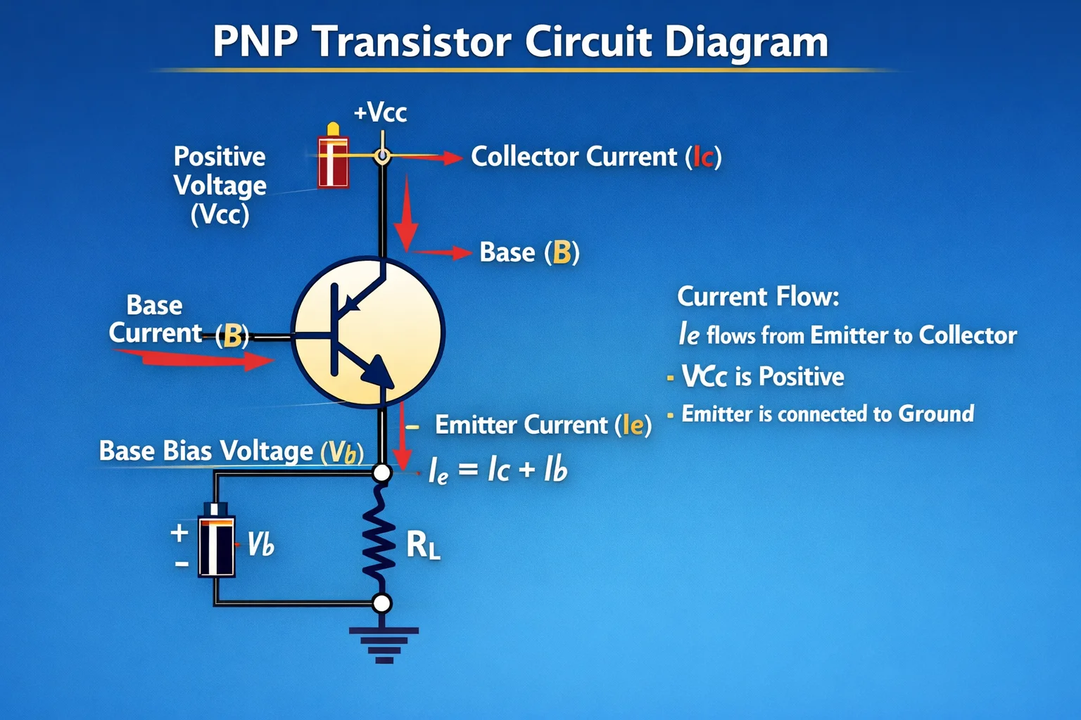
This image comes with a basic PNP transistor circuit diagram that shows current flow in a PNP transistor during ON conditions.
In a circuit, the emitter pin can be seen connected with the positive supply voltage VCC, the collector connected with RL, which is the load resistor, and the base pin receiving control voltage VB.
An arrow over the emitter point inward, denotes the symbol of PNP. If the base voltage is less than the emitter voltage, which is 0.7 for a silicon transistor, the base-emitter junctions are in a forward-bias condition and cause transistor conduction.
It is shown in red arrows: emitter current flows out from the positive supply and goes towards the transistor with the emitter pin. In a transistor, current follows two paths: a small base current ID and a larger current part towards the collector called IC.
Collector current flows through the load resistor and then shifts to ground. That is shown in equation form as IE = IC + IB, so emitter current is equal to the summation of collector and base current.
This circuit also shows a PNP transistor operating differently compared to an NPN transistor since the conventional current direction is from the emitter to collector.
A small current at the base regulates high current flow to the collector. These amplification features make it useful for PNP in switching circuits, amplifiers, power control and also electronic control systems since it offers positive supply switching in this application.
Load resistor RL shows external devices controlled with transistors such as relays and motors.
Comparison: PNP vs. FET
A bipolar PNP transistor needed to be compared with different transistor types having certain requirements. Bipolar PNP transistors are better than field-effect transistors for different methods, like good current gain and fast switching.
For some projects, FETs offer less power usage, a small size, and lower noise levels.
Examples
- Bipolar PNP transistor is commonly used for audio amplifiers for the amplification of audio signals delivered to speakers. For controlling current flow and motor speed in a motor control circuit, a PNP transistor is used.
- Electronic thermometers and thermostats use bipolar PNP transistors for temperature sensors.
|
Parameter |
PNP Transistor (BJT) |
FET (Field Effect Transistor) |
|
Full Form |
Positive-Negative-Positive Transistor |
Field Effect Transistor |
|
Device Type |
Bipolar device |
Unipolar device |
|
Charge Carriers |
Electrons and holes |
Either electrons or holes |
|
Control Method |
Current-controlled device |
Voltage-controlled device |
|
Input Current |
Requires base current |
Gate current is nearly zero |
|
Input Impedance |
Low to medium |
Very high |
|
Output Impedance |
Lower |
Higher |
|
Power Consumption |
Higher due to the base current |
Lower due to negligible gate current |
|
Switching Speed |
Moderate |
Faster, especially MOSFETs |
|
Noise Performance |
Higher noise |
Lower noise |
|
Temperature Stability |
Less stable |
Better thermal stability |
|
Gain Type |
Current gain (β) |
Voltage gain/transconductance |
|
Drive Requirement |
Continuous base current needed |
Voltage at the gate controls operation |
|
Efficiency |
Lower in switching applications |
Higher in switching applications |
|
Common Applications |
Amplifiers, signal processing, and switching circuits |
Power supplies, digital circuits, motor drives, high-speed switching |
|
Symbol Control Terminal |
Base |
Gate |
|
Main Current Path |
Emitter → Collector |
Source → Drain |
|
Integration in ICs |
Less common in modern ICs |
Widely used in CMOS ICs |
|
Switching Losses |
Higher |
Lower |
|
Examples |
PNP BJT (BC557, 2N3906) |
JFET, MOSFET, Power MOSFET |
PNP VS NPN transistor
Basic differences between an NPN and a PNP transistor are as follows:
|
Parameter |
NPN Transistor |
PNP Transistor |
|
Structure |
N-type – P-type – N-type |
P-type – N-type – P-type |
|
Majority Charge Carriers |
Electrons |
Holes |
|
Current Flow Direction |
Collector → Emitter |
Emitter → Collector |
|
Conventional Current Direction |
Collector to Emitter |
Emitter to Collector |
|
Base Bias Requirement |
Base must be positive relative to the emitter |
Base must be negative relative to the emitter |
|
Turn-On Condition |
Base-emitter junction forward biased with positive voltage |
Base-emitter junction is forward-biased with a negative voltage |
|
Symbol Arrow Direction |
The arrow points outward from the emitter |
The arrow points inward toward the emitter |
|
Electron Flow |
Emitter → Collector |
Collector → Emitter |
|
Switching Speed |
Generally faster due to higher electron mobility |
Slightly slower due to hole conduction |
|
Circuit Position |
Commonly used as a low-side switch |
Commonly used as a high-side switch |
|
Power Supply Connection |
Emitter usually connected to ground |
Emitter usually connected to the positive supply |
|
Popularity |
More widely used |
Less commonly used |
|
Typical Applications |
Logic circuits, amplifiers, switching circuits, microcontroller interfacing |
High-side switching, complementary amplifier circuits |
|
Common Examples |
2N2222, BC547, 2N3904 |
2N2907, BC557, 2N3906 |
|
Current Gain (β) |
Similar to PNP counterparts |
Similar to NPN counterparts |
|
Ease of Circuit Design |
Easier in positive-voltage systems |
More complex in positive-voltage systems |
What is the Transistor Effect
A transistor, we know, is a semiconductor component that is part of different devices for on/off to perform sensor applications. It performs amplification of small signals, like the position-sensing element of a proximity switch, for controlling large signals.
That high signal is delivered to the point or devices with proper current rating. Transistors come with PNP AND NPN configurations.
P and N show a semiconductor configuration of PNP and NPN transistor configurations.
How transistors work as switching devices
- Transistors’ common applications as amplifiers and switching circuits. Transistors make solid-state switches where transistors work like a closing switch in the saturation region and an off switch for when they function in the cutoff region.
- Both types of transistors, either NPN or PNP, work as switches. A transistor conducts current through the collector-to-emitter path when voltage is applied at the base point. If the base voltage has a zero value, it means the switch is in the closed state.
- When a reference voltage is given, the base zero-mean switch is open. For transistors working in the cut-off region, PN junctions are reverse-biassed conditions that cause zero input and output current with high voltage over the transistor.
- In switch mode, for transistors working in the saturation region, PN junctions in forward-biassed conditions cause maximum input and output current, and high voltage occurs at the transistor, and it works like a closed switch.
FAQS
Can a PNP transistor replace an NPN transistor?
- Due to different electrical features, PNP transistors are not used as much as NPN transistors. Compared to an NPN transistor, the polarity of the power supply and the current flow direction of a PNP transistor are reversed.
How can I identify the pin configuration of a bipolar PNP transistor?
- The manufacturer's datasheet used for finding the bipolar PNP transistor pin configuration. Transistor pin that shows each pin's operations, shown in the datasheet.
Disclaimer: This post was provided by a guest contributor. Coherent Market Insights does not endorse any products or services mentioned unless explicitly stated.


