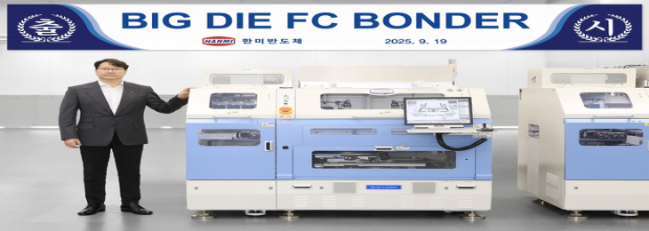
Hanmi Semiconductor expanded its supply of new equipment for AI semiconductors, the Big Die Flip Chip (FC) Bonder, to a global customer. The customer is reported to be one of the global semiconductors back-end packaging (OSAT) companies.
With its dominance in the high-bandwidth memory (HBM) equipment market, the company is now making a full-scale entry into the system semiconductor packaging market.
This product launch is a major transition as it holds Hanmi Semiconductor’s expansion from the memory domain of HBM to the 2.5D packaging market, which consists graphics processing units (GPUs). It effectively throws down the gauntlet to Japanese companies that have dominated the FC bonder market.
The newly releases Big Die FC Bonder lives up to its name: it’s built to handle much larger dies. It supports interposer‑packaging up to 75 mm × 75 mm, greatly exceeding the more typical 20 mm × 20 mm sizes in conventional semiconductor packaging.
This capability is critical for chiplet‑based architectures like those in NVIDIA’s latest AI semiconductors, where multiple dies are integrated side‑by‑side on a single substrate.
Hanmi Semiconductor is preparing for a future where hybrid devices those integrating different types of components (logic, memory, passive elements) and possibly different nodes or substrates, play a central role in system design.
They have also planned customer base expansion. While the main customers for the existing TC bonders were memory semiconductor companies like SK Hynix and Micron, the FC bonder’s core customers are foundries like TSMC and global semiconductor OSAT companies like ASE and Amkor.
Executive Statement
According to Kwak Dong-shin, chairman of Hanmi Semiconductor, they are now able to provide various equipment not only to memory customers but also to IDM and OSAT customers.


