Global 3D Stacking Market Size and Forecast – 2026-2033
The global 3D stacking market is estimated to be valued at USD 2.37 Bn in 2026 and is expected to reach USD 8.83 Bn by 2033, exhibiting a compound annual growth rate (CAGR) of 20.7% from 2026 to 2033.
Key Takeaways of the Global 3D Stacking Market
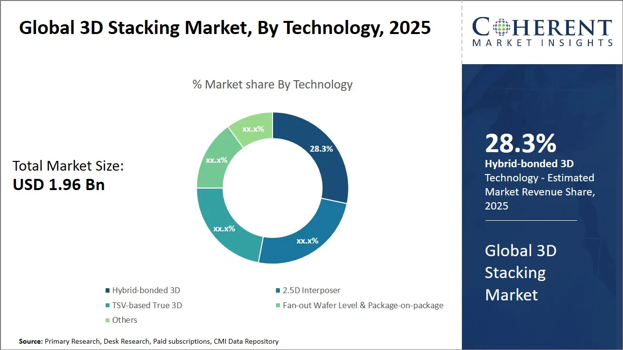
- The hybrid-bonded 3D segment leads the market holding an estimated share of 29.3% in 2026.
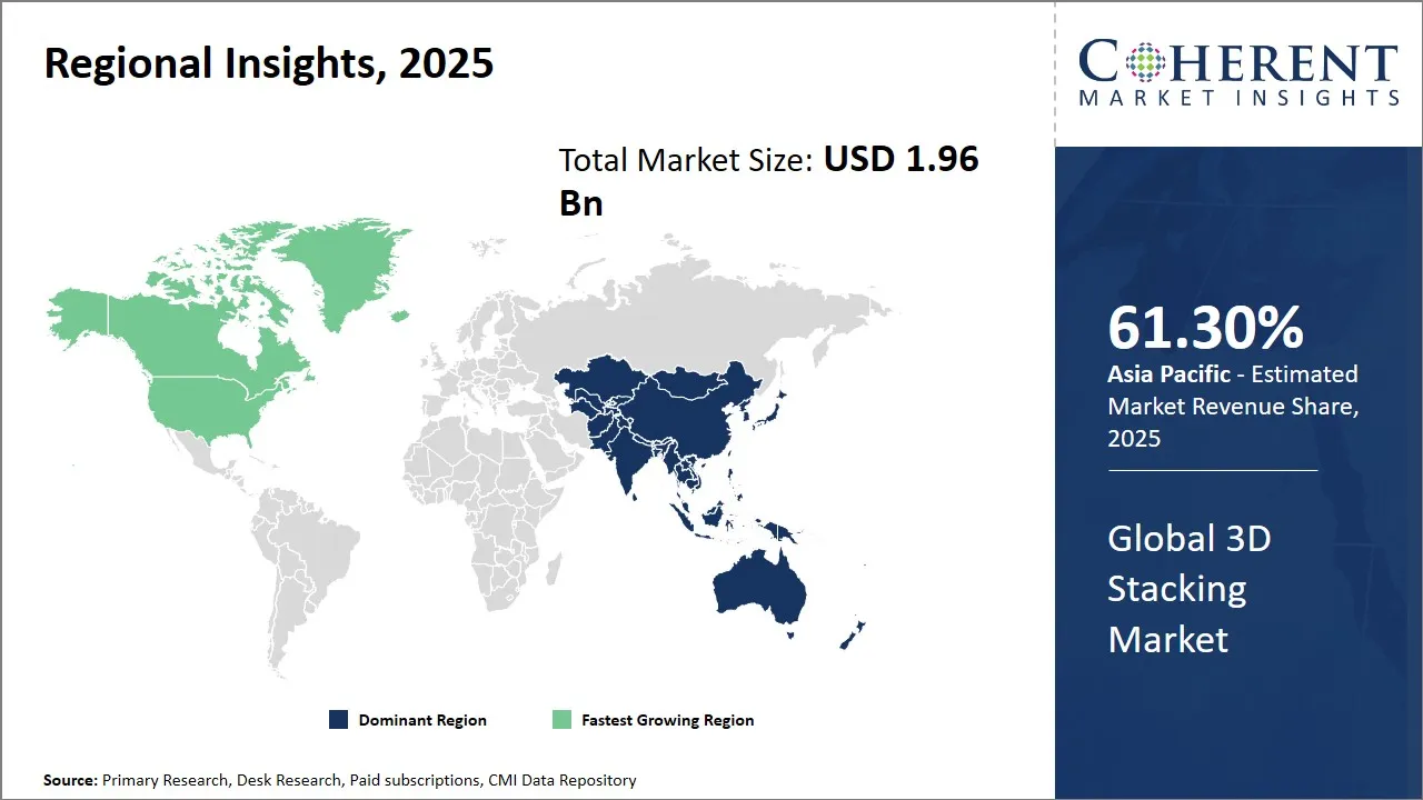
- Asia Pacific is estimated to lead the market with a share of 61.3% in 2026.
- North America, holding a share of 22.4% in 2026, and it is projected to be the fastest growing region.
Market Overview
The market is seeing fast innovation with a focus on integrating heterogeneous components into compact, high-performance packages. Advancements in Through-Silicon Via (TSV) technology and wafer-level packaging are enabling increased data transfer speeds and improved thermal management. Also, growing investments in artificial intelligence, Internet of Things (IoT), and 5G infrastructure are adding to the demand for 3D stacking solutions.
Current Events and Its Impact
|
Current Events |
Description and its impact |
|
TSMC's Advanced Packaging Expansion |
|
|
STMicroelectronics' USD 71 Million (€60 Million) Investment in France |
|
|
Silicon Box's USD 3.79 Billion (€3.2 Billion) Investment in Italy |
|
Uncover macros and micros vetted on 75+ parameters: Get instant access to report
Global 3D Stacking Market Insights, by Technology – Hybrid-bonded 3D Segment Leads Owing to its Superior Integration Capabilities
Hybrid-bonded 3D technology is gaining a lot of popularity in the global 3D stacking market, holding an estimated share of 29.3% in 2026. This technology makes possible the precise alignment and bonding of multiple silicon wafers or dies at an atomic or molecular level. The high-density vertical integration achieved through hybrid bonding improves signal transmission speed and energy efficiency, which is useful for applications needing high processing power combined with low latency. The segment is seeing increasing demand for advanced computing solutions in sectors such as data centers, Artificial Intelligence (AI), and High-Performance Computing (HPC). These applications need high-bandwidth and low-power memory and logic components, which hybrid-bonded 3D stacking makes possible by enabling heterogeneous integration of memory and logic layers.
Also, consumer electronics such as smartphones and wearables benefit from hybrid bonding’s ability to reduce device thickness and footprint while improving computational capabilities. The technique overcomes limitations seen in traditional Through-Silicon Via (TSV) approaches by eliminating the need for large vertical interconnects, thus reducing parasitic capacitance and thermal resistance. Manufacturing advancements and improved yield rates in wafer bonding processes have also added to the adoption of hybrid-bonded 3D stacking. Broadcom has introduced its 3.5D eXtreme Dimension System in Package (XDSiP) platform, which uses hybrid bonding technology to make possible ultra-high-performance processors for AI and HPC workloads. This platform uses face-to-face 3D chip-stacking technology based on hybrid bonding, connecting the pillars of copper wiring on the front of each silicon die directly without solder bumps.
Impact of AI on the 3D Stacking Market
Artificial Intelligence (AI) is influencing the 3D stacking market a lot by improving design processes and making possible the development of more efficient and compact semiconductor devices. AI-driven generative design algorithms allow engineers to explore a multitude of design possibilities, leading to optimized layouts that improve performance and reduce power consumption. This is useful because the demand for high-performance computing (HPC) and artificial intelligence (AI) applications continues to rise, needing advanced packaging solutions that can handle complex workloads efficiently.
An example of AI's impact is ASE Technology Holdings' adoption of AMD's EPYC and Ryzen processors for its server and client systems in June 2025. This transition resulted in a 50% improvement in system performance, a 6.5% reduction in power consumption, and a 30% decrease in total cost of ownership.
Regional Insights

To learn more about this report, Download Free Sample
Asia Pacific 3D Stacking Market Analysis and Trends
The Asia Pacific region, holding a share of 61.3% in 2026, is expected to dominate the 3D stacking market because of its fast expanding semiconductor manufacturing base, favorable governmental initiatives, and large-scale investments in emerging technologies.
The partnerships between foundries like TSMC and Samsung, and packaging specialists add to innovation in 3D stacking. Trade dynamics, including regional supply chain realignment and efforts toward technological self-reliance, add to adoption. These factors, alongside an increasing number of startups and established firms in semiconductor packaging and testing, position Asia Pacific as the fastest-growing market.
North America 3D Stacking Market Analysis and Trends
North America, holding a share of 22.4% in 2026, is expected to exhibit the fastest growth in the global 3D stacking market because of its well-established semiconductor ecosystem, the presence of leading-edge technology companies, strong government support for advanced electronics manufacturing, and a strong supply chain network.
Major players such as Intel, AMD, and Micron Technology are working on 3D stacking innovations, using these technologies in CPUs, memory, and high-performance computing applications. Also, trade policies supporting technological exports and a focus on maintaining semiconductor sovereignty adds to North America’s commanding position. The ecosystem including chip design, fabrication, and packaging facilities adds to fast deployment and commercialization of 3D stacking technologies.
3D Stacking Market Outlook for Key Countries
U.S. 3D Stacking Market Analysis and Trends
The U.S. grows because of its strong innovation landscape led by companies such as Intel, AMD, and Qualcomm. These firms are using 3D stacking in processor designs and memory solutions, targeting data centers, AI, and HPC sectors. Federal initiatives promoting semiconductor manufacturing and research, such as the CHIPS Act, make domestic capabilities stronger. The collaboration between industry and research institutes ensure continuous technological advancements.
China 3D Stacking Market Analysis and Trends
China shows a push toward semiconductor independence, focusing on advanced packaging technologies including 3D stacking. Chinese companies like SMIC and Tianshu Zhixin are escalating investments in manufacturing and R&D. Government policies focusing on “Made in China 2026” and high funding for semiconductor innovations lead to fast infrastructure and capability enhancement. The integration of 3D stacking fulfils the demand for compact, power-efficient chips in consumer electronics, automotive, and AI-driven applications, making China a key competitive hub.
Taiwan 3D Stacking Market Analysis and Trends
Taiwan acts as a wafer foundry powerhouse with companies like TSMC setting global standards in advanced 3D stacking techniques, such as chiplet integration and Through-Silicon Via (TSV) implementation. Its mature ecosystem of semiconductor fabrication, testing, and packaging adds to fast adoption of 3D stacking. Government support aligned with private sector innovations makes sure Taiwan remains useful for supply chain stability and technology evolution in this segment.
South Korea 3D Stacking Market Analysis and Trends
South Korea 3D stacking market thrives with Samsung and SK Hynix actively advancing 3D stacking for memory and logic chips, targeting next-generation mobile and computing devices. The country sees a strong industrial base, government R&D subsidies, and close integration between chip design and manufacturing entities. South Korea’s high focus on semiconductor leadership adds to continuous improvements in chip density, performance, and energy efficiency enabled by 3D stacking methods.
Japan 3D Stacking Market Analysis and Trends
Japan stands out because of its strengths in materials, equipment, and high-precision manufacturing technologies essential for 3D stacking production. Companies like Sony and Renesas add to specialized applications in automotive electronics, sensors, and industrial solutions. Public-private partnerships and government incentives add to innovation in packaging architectures and integration methods, making Japan’s role stronger in the global semiconductor value chain.
Market Players, Key Development, and Competitive Intelligence

To learn more about this report, Download Free Sample
Top Strategies Followed by 3D Stacking Market Players
- Established players dominate the market by heavily investing in research and development to drive innovation and create high-performance 3D stacking products.
- TSMC, committed to a USD 100 billion investment to establish three new advanced semiconductor plants and an R&D center in the U.S.
- Mid-level players in the 3D stacking market adopt a distinct strategy centered on delivering cost-effective solutions that strike a balance between quality and affordability.
- ASE Technology Holdings’ Integrated Design Ecosystem (IDE) is a platform that enables efficient chip packaging design, reducing cycle time by up to 50% and lowering costs for customers.
- Small-scale players in the global 3D stacking market differentiate themselves by focusing on niche segments or highly specialized features that larger competitors may overlook.
- d-Matrix, developed the Pavehawk chip featuring 3D stacked digital in-memory compute (3DIMC) technology, targeting AI inference workloads. This specialized approach aims to outperform traditional High Bandwidth Memory (HBM) solutions in speed and energy efficiency.
Key Developments
- In May 2025, Advanced Semiconductor Engineering, Inc. (ASE), a member of ASE Technology Holding Co., Ltd., announced Fan-Out Chip-on-Substrate-Bridge (FOCoS-Bridge) with Through Silicon Via (TSV), propelling technology enablement for artificial intelligence (AI) and its pervasive impact on global life.
- In December 2024, Broadcom Inc. announced the availability of its 3.5D eXtreme Dimension System in Package (XDSiP) platform technology, enabling consumer AI customers to develop next-generation custom accelerators (XPUs). The 3.5D XDSiP integrates more than 6000 mm2 of silicon and up to 12 high bandwidth memory (HBM) stacks in one packaged device to enable high-efficiency, low-power computing for AI at scale.
- In November 2024, Lightmatter, the leader in photonic supercomputing, announced a strategic partnership with Amkor Technology, a provider of semiconductor packaging and test services, to create the largest-ever 3D-packaged chip complex utilizing Lightmatter’s innovative Passage platform. This collaboration harnesses Lightmatter’s 3D-stacked photonic engine along with Amkor’s advanced multi-die packaging expertise to meet the interconnect scaling and power demands of today’s Artificial Intelligence (AI) workloads.
- In September 2024, Broadcom completed the successful bring-up of Industry’s first Face-to-Face 3D SoIC. This device uses TSMC’s 5nm Process, 3D die-stacking, and CoWoS packaging technologies to integrate 9x die(s) and 6x HBM stacks in a large package.
Market Report Scope
3D Stacking Market Report Coverage
| Report Coverage | Details | ||
|---|---|---|---|
| Base Year: | 2025 | Market Size in 2026: | USD 2.37 Bn |
| Historical Data for: | 2020 To 2024 | Forecast Period: | 2026 To 2033 |
| Forecast Period 2026 to 2033 CAGR: | 20.7% | 2033 Value Projection: | USD 8.83 Bn |
| Geographies covered: |
|
||
| Segments covered: |
|
||
| Companies covered: |
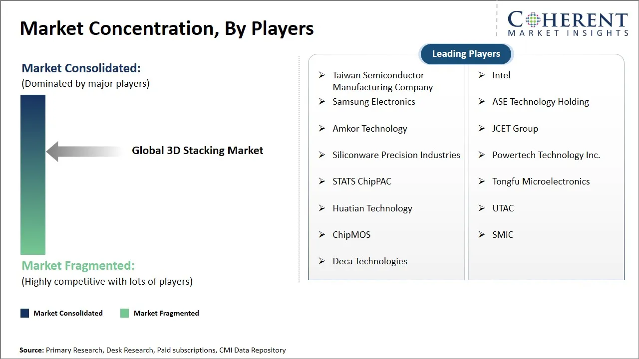
Taiwan Semiconductor Manufacturing Company, Intel, Samsung Electronics, ASE Technology Holding, Amkor Technology, JCET Group, Siliconware Precision Industries, Powertech Technology Inc., STATS ChipPAC, Tongfu Microelectronics, Huatian Technology, UTAC, ChipMOS, SMIC, and Deca Technologies |
||
| Growth Drivers: |
|
||
| Restraints & Challenges: |
|
||
Uncover macros and micros vetted on 75+ parameters: Get instant access to report
Market Dynamics

To learn more about this report, Download Free Sample
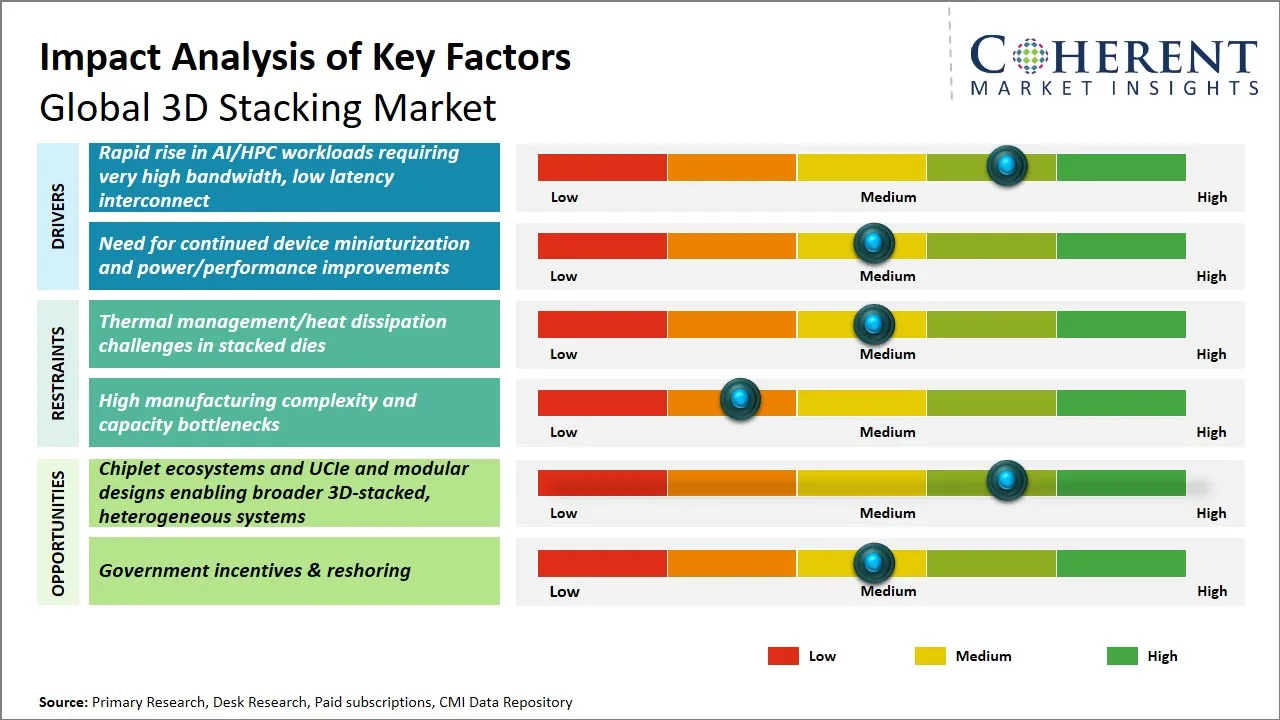
Global 3D Stacking Market Driver - Rapid Rise in AI/HPC Workloads Requiring Very High Bandwidth, Low Latency Interconnect
The rapid expansion of Artificial Intelligence (AI) and High-Performance Computing (HPC) workloads is fueling the need for advanced semiconductor packaging solutions that can deliver exceptionally high bandwidth and ultra-low latency communication between processing units. As AI models grow more complex and compute-intensive, traditional 2D chip architectures struggle to meet the stringent requirements of data throughput and energy efficiency. This has led to a surge in adoption of 3D stacking technologies, which enable vertical integration of multiple dies in a compact form factor, significantly reducing the distance data must travel and thereby minimizing signal delay.
For instance, Microsoft Azure leverages InfiniBand interconnects in its HB-series and N-series virtual machines to support High-Performance Computing (HPC) and AI workloads. The inherent ability of 3D stacking to support heterogeneous integration also allows for seamless combination of memory, logic, and specialized AI accelerators, facilitating faster data exchange and improved performance.
Global 3D Stacking Market Opportunity – Expansion of Chiplet Ecosystems and UCIe Standards Driving Modular 3D-Stacked Heterogeneous Systems
The emergence of chiplet ecosystems combined with the Universal Chiplet Interconnect Express (UCIe) standard presents a significant opportunity in the global 3D stacking market by enabling more versatile and scalable modular designs. Traditional monolithic chip manufacturing faces escalating complexity and cost challenges, making chiplets—small, functional chip blocks—an efficient alternative for building advanced semiconductor systems.
The adoption of 3D stacking technology in chiplet-based architectures allows for vertical integration of heterogeneous components such as logic, memory, and specialized accelerators, optimizing performance and power efficiency. For instance, AMD's MI300A is an Accelerated Processing Unit (APU) designed for AI and HPC applications. It utilizes a chiplet-based architecture, combining multiple chiplets on a single interposer using advanced packaging technologies like CoWoS and InFO. UCIe, as an open standard interconnect, facilitates seamless communication between chiplets from multiple vendors, accelerating ecosystem collaboration and innovation. The modular nature also lowers the barrier to entry for smaller players, fostering a more competitive and dynamic 3D stacking market.
Analyst Opinion (Expert Opinion)
- The surge in AI and HPC workloads is significantly propelling the demand for 3D stacking technologies. These applications require high-bandwidth, low-latency interconnects to manage vast data volumes efficiently. 3D stacking, particularly through technologies like Through-Silicon Vias (TSVs) and hybrid bonding, offers reduced signal travel distances, enhancing processing speeds and energy efficiency.
- The consumer electronics sector is a significant contributor to the 3D stacking market. Devices such as smartphones, wearables, and AR/VR gadgets demand compact, high-performance semiconductors. 3D stacking enables the integration of multiple components, like memory and logic, into a smaller footprint, meeting the industry's need for miniaturization without compromising performance. For example, the adoption of 3D NAND memory in smartphones has increased, with approximately 35% of premium smartphones featuring this technology by 2023.
- The automotive and industrial sectors are increasingly adopting 3D stacking technologies to meet the demands of Advanced Driver-Assistance Systems (ADAS) and industrial automation. These applications require components that offer high reliability, thermal management, and power efficiency. 3D stacking facilitates the integration of sensors, processors, and memory in a compact and efficient manner, essential for the performance of autonomous vehicles and industrial equipment.
Market Segmentation
- Technology Insights (Revenue, USD Bn, 2021 - 2033)
- Hybrid-bonded 3D
- 5D Interposer
- TSV-based True 3D
- Fan-out Wafer Level & Package-on-package
- Others
- Regional Insights (Revenue, USD Bn, 2021 - 2033)
- North America
- U.S.
- Canada
- Latin America
- Brazil
- Argentina
- Mexico
- Rest of Latin America
- Europe
- Germany
- U.K.
- Spain
- France
- Italy
- Russia
- Rest of Europe
- Asia Pacific
- China
- India
- Japan
- Australia
- South Korea
- ASEAN
- Rest of Asia Pacific
- Middle East
- GCC Countries
- Israel
- Rest of Middle East
- Africa
- South Africa
- North Africa
- Central Africa
- North America
- Key Players Insights
- Taiwan Semiconductor Manufacturing Company
- Intel
- Samsung Electronics
- ASE Technology Holding
- Amkor Technology
- JCET Group
- Siliconware Precision Industries
- Powertech Technology Inc.
- STATS ChipPAC
- Tongfu Microelectronics
- Huatian Technology
- UTAC
- ChipMOS
- SMIC
- Deca Technologies
Sources
Primary Research Interviews
Stakeholders
- Semiconductor Foundries and IDMs
- OSAT Companies
- Chiplet Designers and IP Vendors
- AI & HPC System Integrators
- Semiconductor Equipment Manufacturers
- Government Semiconductor and Technology Policy Advisors
Databases
- IEEE Xplore Digital Library
- Semiconductor Industry Association (SIA) Reports
- Global Semiconductor Alliance (GSA) Database
- World Semiconductor Trade Statistics (WSTS)
Magazines
- Semiconductor Today
- 3D InCites
- Chip Scale Review
- Electronics Packaging & Production
Journals
- Journal of Microelectronics and Packaging
- IEEE Transactions on Components, Packaging, and Manufacturing Technology
- Microelectronics Reliability Journal
- Advanced Packaging and Interconnect Journal
Newspapers/News Outlets
- The Semiconductor Times
- EE Times
- The Verge – Semiconductor Section
- Financial Times – Technology Section
Associations
- International Microelectronics Assembly and Packaging Society (IMAPS)
- Semiconductor Equipment and Materials International (SEMI)
- Global Advanced Packaging Consortium (GAPC)
- Open Compute Project (OCP) for advanced packaging standards
Public Domain Sources
- United States International Trade Commission (USITC)
- European Commission – DG CONNECT Reports
- World Intellectual Property Organization (WIPO) Patent Database
- United Nations Industrial Development Organization (UNIDO)
Proprietary Elements
- CMI Data Analytics Tool, Proprietary CMI Existing Repository of information for last 8 years
Share
Share
About Author
As an accomplished Senior Consultant with 7+ years of experience, Pooja Tayade has a proven track record in devising and implementing data and strategy consulting across various industries. She specializes in market research, competitive analysis, primary insights, and market estimation. She excels in strategic advisory, delivering data-driven insights to help clients navigate market complexities, optimize entry strategies, and achieve sustainable growth.
Missing comfort of reading report in your local language? Find your preferred language :
Transform your Strategy with Exclusive Trending Reports :
Frequently Asked Questions
EXISTING CLIENTELE
Joining thousands of companies around the world committed to making the Excellent Business Solutions.
View All Our Clients

