

Global Screen Mask Market Size and Forecast – 2026 To 2033
The global screen mask market is expected to grow from USD 1.45 Bn in 2026 to USD 2.40 Bn by 2033, registering a compound annual growth rate (CAGR) of 5% from 2026 to 2033. The global screen mask market is driven by the growing demand for high-resolution photomasks for IC fabrication. On July 2, 2026, Intel announced that it has initiated the expansion of its Bowers Campus in California, U.S. in a bid to produce more photomasks (reticles) in the U.S.
Key Takeaways of the Global Screen Mask Market
- The quartz screen masks segment is expected to account for 41.0 % of the global screen mask market share in 2026. Expansion of automotive electronics and display applications is driving the growth of the quartz screen masks segment. On July 4, 2024, LG Electronics launched a new series of ultra-thin, curved, and transparent OLED automotive displays developed for premium digital cockpit applications, targeting next-generation vehicle manufacturers.
- The binary masks segment is estimated to capture 39.0 % of the market share in 2026. Growing demand for consumer electronics and smart devices is majorly driving the growth of the segment. On June 17, 2026, Google announced the release of its new Google Home Speaker with Gemini AI integration, continuing the trend of AI-enabled smart home products that are driving the demand for advanced consumer electronics chips.
- The semiconductor manufacturing segment is estimated to capture 44.0 % of the market share in 2026. Increasing investments in next-generation chip fabrication facilities is driving the growth of the segment. On March 4, 2025, TSMC announced its intention to expand its investment in advanced semiconductor manufacturing in the U.S. by an additional USD 100 billion.
- Asia Pacific is expected to dominate the screen mask market in 2026 with a market share of 47.0 %. Expansion of semiconductor fabrication plants across Asia Pacific is driving the growth of the regional market. SK hynix announced that it would invest an additional USD 64 billion in its Cheongju, South Korea campus to expand the production of 3D NAND and high-bandwitch memory packaging at the site.
- North America is expected to account for 26.0 % share in 2026 and is projected to record the fastest growth over the forecast period. Rising adoption of flexible and foldable display panels for consumer electronics in North America is driving the growth of the regional market. On August 20, 2025, Google announced its second-generation foldable smartphone, the Pixel 10 Pro Fold, equipped with a more flexible OLED display.
- The adoption of extreme ultraviolet (EUV) mask technology: The use of EUV mask technology is transforming advanced semiconductor manufacturing as chipmakers move to high-precision screen masks that can support sub-5 nm process nodes, while improving pattern accuracy and production efficiency.
- Increasing production of OLED, MicroLED and foldable displays: The growing production rates of OLED and MicroLED displays is increasing the demand for high-resolution masks to enable advanced display manufacturing is accelerating. To deliver higher display performance, these new electronic display technologies require ultra-fine patterning and tighter dimensional control.
Segmental Insights
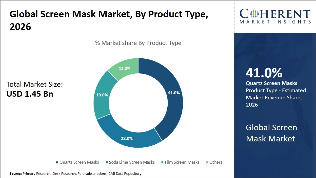
Why Do Quartz Screen Masks Dominate the Global Screen Mask Market?
The quartz screen masks segment is expected to account for 41.0% of the global screen mask market share in 2026. The widespread adoption of quartz screen masks is primarily attributed to their exceptional dimensional stability and optical transparency in advanced photolithography processes. Quartz substrates offer minimal thermal expansion and UV radiation resistance, allowing for exceptionally accurate pattern transfer even when repeatedly subjected to high temperatures. The qualities of quartz make it a necessity for the fabrication of cutting edge semiconductor devices, high resolution display panels, and precision electronic components where even minuscule pattern errors may alter device performance and production yield. On October 2, 2025, HOYA expanded the development of next-generation EUV photomask blanks manufactured from ultra-high-purity quartz substrates to improve defect control and support advanced semiconductor process nodes. (Source: HOYA)
- Current Industry Events of 2026
- Market Size Estimation
- Regional Breakdown
- Competitive Landscape
- Customer Intelligence
- Segmental Analysis
- Pricing Analysis
- Key Market Drivers, Challenges & Future Trends
- Customized Insights Section
Why are Binary Masks the Most Preferred Technology Type?
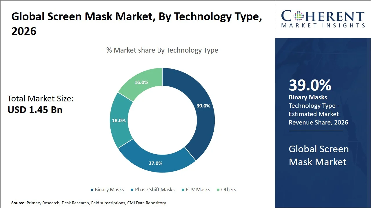
The binary masks segment is expected to account for 39.0% of the global screen mask market share in 2026. The primary factor driving the widespread preference for binary masks is their cost-effective manufacturing and broad compatibility with mature semiconductor fabrication processes. Binary masks have a simple design with transparent and opaque areas making them easier and cheaper to manufacture than phase shift or extreme ultraviolet masks, while yet providing dependable pattern fidelity for a large variety of integrated circuits and display applications. They are the first choice for many typical semiconductor and electronics production environments because of their established performance, quicker production cycles, and adaptability for high-volume manufacture. For example, Photronics, Inc. is a leading manufacturer of binary masks.
Semiconductor Manufacturing Dominates the Global Screen Mask Market
The semiconductor manufacturing segment is expected to account for 44.0% of the global screen mask market share in 2026. The dominant position of semiconductor production is mainly driven by the industry’s continual move to lower process nodes and increased chip complexity, which demand highly precise screen masks for accurate photolithography. Photomasks are used to transfer very fine circuit layouts on silicon wafers with extraordinary precision during all phases of the integrated circuit fabrication process. With the demand for processors, memory chips, artificial intelligence accelerators, and automotive semiconductors continuing to grow, semiconductor manufacturers are spending heavily in sophisticated mask technologies to boost yield, eliminate defects and satisfy tight production standards.
Currents Events and their Impact
Current Events | Description and its Impact |
European Chips Act (European Union, 2025 implementation) |
|
U.S. CHIPS and Science Act |
|
Screen Mask Market Dynamics
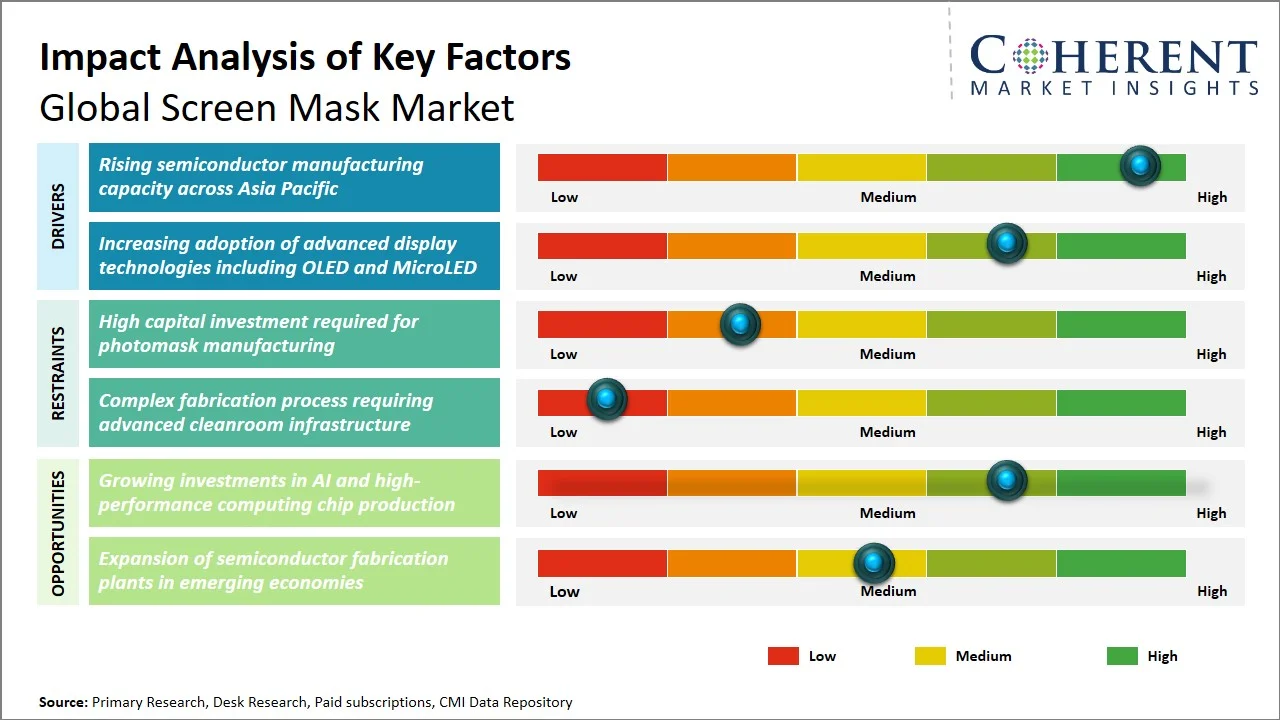
Market Drivers
- Rising semiconductor manufacturing capacity across Asia Pacific: The fast-growing semiconductor manufacturing capacity in the Asia Pacific region is driving the demand for screen masks used in photolithography and wafer fabrication procedures. Countries such as China, Taiwan, South Korea, Japan, India and Singapore are pouring billions into new fabrication factories and expanding existing facilities to meet increased demand for artificial intelligence chips, automotive semiconductors, memory devices and consumer electronics. The region’s manufacturing expansion is a key driver of continued demand for advanced quartz, binary and EUV-compatible screen masks, as each new production line requires high-precision screen masks to accurately transfer circuit patterns. On January 27, 2026, Micron Technology, Inc. broke ground on an advanced wafer fabrication facility located within the company's existing NAND manufacturing complex in Singapore. This new facility represents a planned investment of approximately USD 24 billion over 10 years and is designed to ultimately provide 700,000 square feet of cleanroom space. (Source: Micron Technology)
- Increasing adoption of advanced display technologies including OLED and MicroLED: The growth in the adoption of advanced display technologies such as OLED and MicroLED is supporting the demand for precision screen masks that can produce very precise and complex display patterns. For making these future generation display technologies we need higher photolithography accuracy for making high resolution pixels, lower bezels and flexible panel designs and also keeping the performance uniform across huge substrates. With the development in production of smartphones, televisions, wearables, automotive displays and augmented reality products based on OLED and MicroLED panels, the investments in advanced screen mask technologies to fulfill the demanding manufacturing requirements are also increasing. On December 26, 2025, LG introduced UltraGear evo Gaming Monitor range, featuring Next-Generation Tandem OLED Technology, which includes a curved 5K2K OLED gaming monitor for high-end gaming and professional use.
Emerging Trends
- Integration of artificial intelligence and automated inspection systems: Integration of artificial intelligence is boosting mask manufacture by providing real-time defect identification, predictive maintenance, and process optimization, decreasing production errors while improving yield and manufacturing consistency.
- Expansion of regional semiconductor manufacturing ecosystems: Expansion of regional semiconductor manufacturing ecosystem is driving investment in local photomask manufacturing facilities, with government incentives and supply chain localization efforts to build manufacturing resilience and reduce dependency on foreign suppliers.
Regional Insights
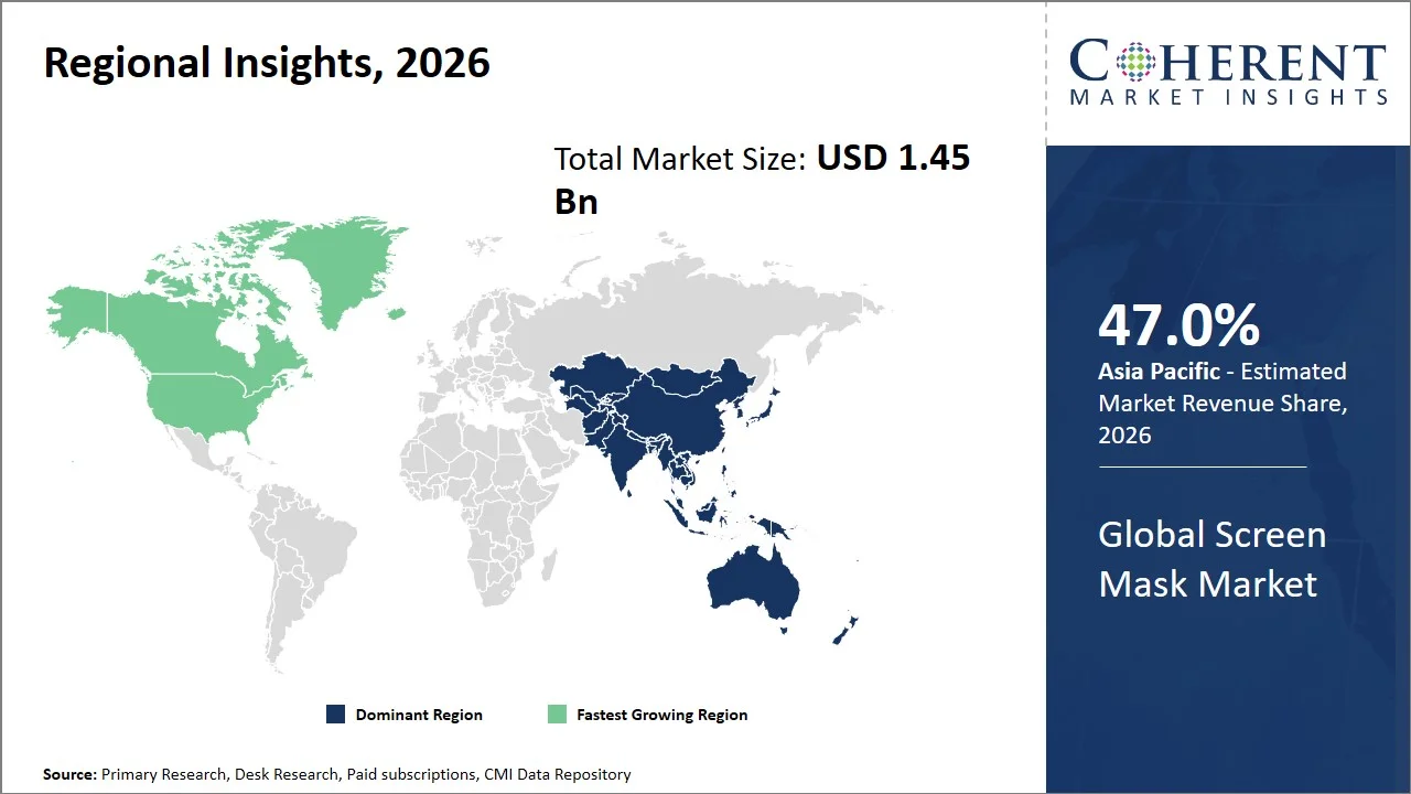
Why is Asia Pacific a Strong Market for Screen Masks?
Asia Pacific is expected to account for a market share of 47.0% in 2026. Asia Pacific is the production hub for screen masks in the world, owing to the presence of modern semiconductor foundries and display panel makers. Leading chip fabrication facilities in Taiwan, South Korea, Japan and China require high-precision quartz and EUV-compatible masks to produce sophisticated logic and memory. The region also has broad OLED and MicroLED production by Samsung Display, LG Display, BOE and AUO, providing continuous demand for screen masks used in semiconductor and flat panel display fabrication.
Why Does the North America Screen Mask Market Exhibit High Growth?
North America is projected to account for 26.0% of the global screen mask market and is expected to register the fastest growth. North America is marked by a strong need for innovative screen masks that enable leading-edge semiconductor manufacturing, research, and defense electronics. Procurement of high-resolution photomasks for advanced process technologies has expanded with the growth of new wafer fabrication plants by businesses like as Intel, GlobalFoundries and Texas Instruments. The region boasts a robust ecosystem of semiconductor equipment vendors and providers of photomask inspection technologies, helping to accelerate the pace of innovation in mask manufacturing and quality control.
Global Screen Mask Market Outlook for Key Countries
Why is China Emerging as a Major Hub in the Screen Mask Market?
China's domestic usage of screen masks is increasing due to significant expenditures in semiconductor self-sufficiency and display manufacture. Local foundries and display manufacturers are ramping up purchase of advanced masks as new fabrication facilities come online as part of national semiconductor development projects. Additionally, the mass production of LCD, OLED and developing MicroLED panels in the country also drives consistent need for high-precision screen masks in consumer electronics, automotive displays and industrial applications.
Is U.S. the Next Growth Engine for the Screen Mask Market?
The U.S. screen mask market is being propelled by investments in advanced semiconductor fabrication, artificial intelligence processors, aerospace electronics and high-performance computer devices. Domestic chip makers are building advanced production capability that demands complex binary, phase shift and EUV masks to accommodate increasingly complex integrated circuit designs. The presence of top semiconductor design businesses and photolithography equipment developers further enhances the demand for technologically superior screen masks.
Taiwan Screen Mask Market Analysis and Trends
Taiwan is one of the most strategically important markets since it hosts the world’s greatest concentration of advanced semiconductor foundries making cutting-edge chips. Continuous investments are made to achieve very high precision photomasks for next-generation process technologies that can preserve pattern fidelity at advanced process nodes. Mature semiconductor supply chain, specialized mask fabrication capabilities, and strong integration between foundries and photomask providers facilitate ongoing technical innovation and high production volumes.
Japan Screen Mask Market Analysis and Trends
The market for screen masks in Japan is strategically important due to the presence of one of the world’s most advanced photomask manufacturing ecosystem and a strong position in semiconductor materials and lithography technologies. Domestic suppliers of high-precision quartz photomasks used in the fabrication of advanced logic, memory, image sensors and power semiconductors include Toppan Holdings, Dai Nippon Printing, HOYA and SK-Electronics Japan. The country’s growing investment in next-generation semiconductor manufacturing, including the Rapidus advanced chip project in Hokkaido and continued production by Renesas and Kioxia, is driving demand for EUV-compatible masks and ultra-high-precision photomask inspection technologies for leading-edge fabrication processes.
South Korea Screen Mask Market Analysis and Trends
South Korea is the leader in memory semiconductor production and high-end OLED display manufacture, thus demand for screen masks should be robust there. Advanced DRAM, NAND flash and system semiconductor manufacture needs very precise masks that can handle the complicated circuit designs. The large-scale production of OLED panels for smartphones, televisions and automotive displays adds to the demand for high-resolution display masks. Continuous investment in next-generation semiconductor technology further strengthens the country’s market position.
Global Screen Mask Market - Semiconductor Node Migration Impact on Mask Complexity
Semiconductor Process Node | Typical Production Period | Relative Mask Complexity | Typical Number of Mask Layers per Chip |
≥65 nm | Mature production | Low | 20-35 |
45–28 nm | High-volume production | Moderate | 30-45 |
22–16 nm | Advanced production | Moderately High | 45-60 |
10–7 nm | Leading-edge production | High | 60-80 |
5–3 nm | Advanced leading-edge | Very High | 80-100 |
2 nm and Below | Emerging commercial production | Ultra-High | 100-120 |
How is Growing Investments in AI and High-Performance Computing Chip Production Creating New Growth Opportunities in the Screen Mask Market?
Growing investments in artificial intelligence and high performance computing chip fabrication are offering major growth opportunities for the screen mask market. This is because of the rising demand for highly advanced photomasks that can cope with sophisticated semiconductor process nodes and complex chip designs. The need for high-precision quartz, phase shift and EUV compatible screen masks is growing because to the complex circuit layouts and very tight dimensional tolerances required for AI accelerators, graphics processors and data center CPUs. With semiconductor manufacturers ramping up fabrication capacity to support increasing demand for AI infrastructure, advanced computing platforms and even cloud services, investment in next-generation screen mask production, inspection and defect control technologies continue to ramp up.
On July 18, 2025, Rapidus Corporation announced that prototyping has started for its 2nm gate-all-around (GAA) transistor structure at Rapidus’ Innovative Integration for Manufacturing (IIM-1) foundry. The prototype wafers also started to obtain their electrical characteristics. (Source: Rapidus)
Market Players, Key Development, and Competitive Landscape
Key Developments
- On October 31, 2025, Lasertec Corporation announced the release of the ACTIS A200HiT series. The new system delivers a significant enhancement in productivity for EUV mask quality assurance at wafer fabs.
- On February 7, 2024, Toppan Photomask announced that it has entered into a joint research and development agreement with IBM related to the 2 nanometer (nm) logic semiconductor node, using extreme ultraviolet (EUV) lithography. This agreement also includes High-NA EUV photomask development capability on next-generation semiconductors.
Competitive Landscape
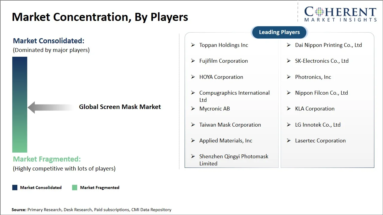
The global screen mask market is characterized by a highly concentrated competitive environment with technological capabilities, pattern precision and process yield determining market positioning. Established producers such as Toppan Holdings, Dai Nippon Printing, HOYA, SK-Electronics, Photronics and Taiwan Mask Corporation continue to develop superior photomask portfolios for EUV lithography, high resolution display panels and advanced packaging applications. The contest is becoming more and more oriented around defect-free mask production, ultra-flat quartz substrates, high-precision electron-beam writing and automated mask-inspection systems.
Market Report Scope
Screen Mask Market Report Coverage
| Report Coverage | Details | ||
|---|---|---|---|
| Base Year: | 2025 | Market Size in 2026: | USD 1.45 Bn |
| Historical Data for: | 2020 To 2024 | Forecast Period: | 2026 To 2033 |
| Forecast Period 2026 to 2033 CAGR: | 5% | 2033 Value Projection: | USD 2.40 Bn |
| Geographies covered: |
| ||
| Segments covered: |
| ||
| Companies covered: | Toppan Holdings Inc, Dai Nippon Printing Co., Ltd, Fujifilm Corporation, SK-Electronics Co., Ltd, HOYA Corporation, Photronics, Inc, Compugraphics International Ltd, Nippon Filcon Co., Ltd, Mycronic AB, KLA Corporation, Taiwan Mask Corporation, LG Innotek Co., Ltd, Applied Materials, Inc, Lasertec Corporation, and Shenzhen Qingyi Photomask Limited | ||
| Growth Drivers: |
| ||
| Restraints & Challenges: |
| ||
Analyst Opinion (Expert Opinion)
- Rapid advancements in semiconductor manufacturing technologies, rather than production volume growth alone, is driving the evolution of the screen mask market. As chip geometries get smaller and smaller, more and more attention is being placed on mask accuracy, defect reduction and compatibility with modern lithography methods. The flow of investments into EUV-ready photomask production, next-generation inspection systems, and localized manufacturing capabilities is driven by the need to meet the ever more exacting quality requirements of the world’s major semiconductor foundries and integrated device makers.
- The screen mask market will witness continued technology development, as semiconductor manufacture moves towards more sophisticated device architectures, advanced packaging, and the integration of heterogeneous chips. Photomasks with higher pattern density and tighter dimensional control will be demanded due to the use of artificial intelligence processors, high-bandwidth memory, automotive semiconductors and MicroLED displays.
- Regional semiconductor manufacturing investments in North America, Europe, Japan, India and Southeast Asia are likely to create a more diversified global supply chain. Continued innovation in EUV lithography, computational mask optimization and automated defect inspection are expected to redefine competitive differentiation over the next few years.
Speak to the analyst
Want personalized insights?
Take the findings above to one of our principal consultants, or have the report rebuilt around the segments, geographies and competitors you actually track.
Market Segmentation
- Product Type Insights (Revenue, USD Billion, 2021 - 2033)
- Quartz Screen Masks
- Soda Lime Screen Masks
- Film Screen Masks
- Others
- Technology Type Insights (Revenue, USD Billion, 2021 - 2033)
- Binary Masks
- Phase Shift Masks
- EUV Masks
- Others
- Application Insights (Revenue, USD Billion, 2021 - 2033)
- Semiconductor Manufacturing
- Flat Panel Displays
- Printed Circuit Boards
- MEMS Devices
- Optoelectronics
- Regional Insights (Revenue, USD Billion, 2021 - 2033)
- North America
- U.S.
- Canada
- Latin America
- Brazil
- Argentina
- Mexico
- Rest of Latin America
- Europe
- Germany
- U.K.
- Spain
- France
- Italy
- Russia
- Rest of Europe
- Asia Pacific
- China
- India
- Japan
- Australia
- South Korea
- ASEAN
- Rest of Asia Pacific
- Middle East
- GCC Countries
- Israel
- Rest of Middle East
- Africa
- South Africa
- North Africa
- Central Africa
- North America
- Key Players Insights
- Toppan Holdings Inc
- Dai Nippon Printing Co., Ltd
- Fujifilm Corporation
- SK-Electronics Co., Ltd
- HOYA Corporation
- Photronics, Inc
- Compugraphics International Ltd
- Nippon Filcon Co., Ltd
- Mycronic AB
- KLA Corporation
- Taiwan Mask Corporation
- LG Innotek Co., Ltd
- Applied Materials, Inc
- Lasertec Corporation
- Shenzhen Qingyi Photomask Limited
Sources
Primary Research Interviews
- Screen Mask Manufacturers
- Semiconductor Equipment Suppliers
- Electronics OEM Companies
- Photolithography Process Engineers
Magazines
- Semiconductor Digest
- Electronic Design Magazine
- Solid State Technology Magazine
- Advanced Packaging Magazine
Journals
- Journal of Vacuum Science & Technology
- Journal of Micro/Nanolithography, MEMS, and MOEMS
- IEEE Transactions on Semiconductor Manufacturing
Associations
- SEMI (Semiconductor Equipment and Materials International)
- International Electronics Manufacturing Initiative (iNEMI)
- Japan Semiconductor Equipment Association (JSEA)
- Semiconductor Industry Association (SIA)
Public Domain Sources
- U.S. International Trade Commission (USITC) Reports
- World Semiconductor Trade Statistics (WSTS)
- European Commission – Electronics & Semiconductor Industry Reports
- U.S. Patent and Trademark Office (USPTO) – Screen Mask Patent Filings
Proprietary Elements
- CMI Data Analytics Tool
- Proprietary CMI Existing Repository of Information for the last 10 years
Get access to 250+ pages report
Every segment, forecast, competitor profile and data table behind the analysis above — available for instant download.
- ESOMAR Member
- ISO 9001:2015 Certified
- D-U-N-S Registered
- GDPR & CCPA Compliant
Missing comfort of reading report in your local language? Find your preferred language:
Transform your Strategy with Exclusive Trending Reports
Frequently Asked Questions
The global screen mask market is expected to stand at USD 1.45 Bn in 2026 and is expected to reach USD 2.40 Bn by 2033.
The CAGR of the global screen mask market is projected to be 5% from 2026 to 2033.
Rising semiconductor manufacturing capacity across Asia Pacific and increasing adoption of advanced display technologies including OLED and MicroLED are the major factors driving the growth of the global screen mask market.
EUV lithography increases the demand for highly sophisticated masks with extremely low defect levels.
They enable precise pattern formation needed for high-resolution OLED panels.
In terms of product type, the quartz screen masks segment is estimated to dominate the market revenue share in 2026.
High capital investment required for photomask manufacturing and complex fabrication process requiring advanced cleanroom infrastructure are the major factors hampering the growth of the global screen mask market.