Global Surface Analysis Market Size and Forecast – 2026-2033
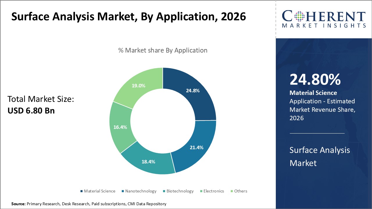
The Gobal Surface Analysis Market is estimated to be valued at USD 6.80 Bn in 2026 and is expected to reach USD 9.81 Bn by 2033, exhibiting a compound annual growth rate (CAGR) of 5.4% from 2026 to 2033.
Key Takeaways of the Surface Analysis Market
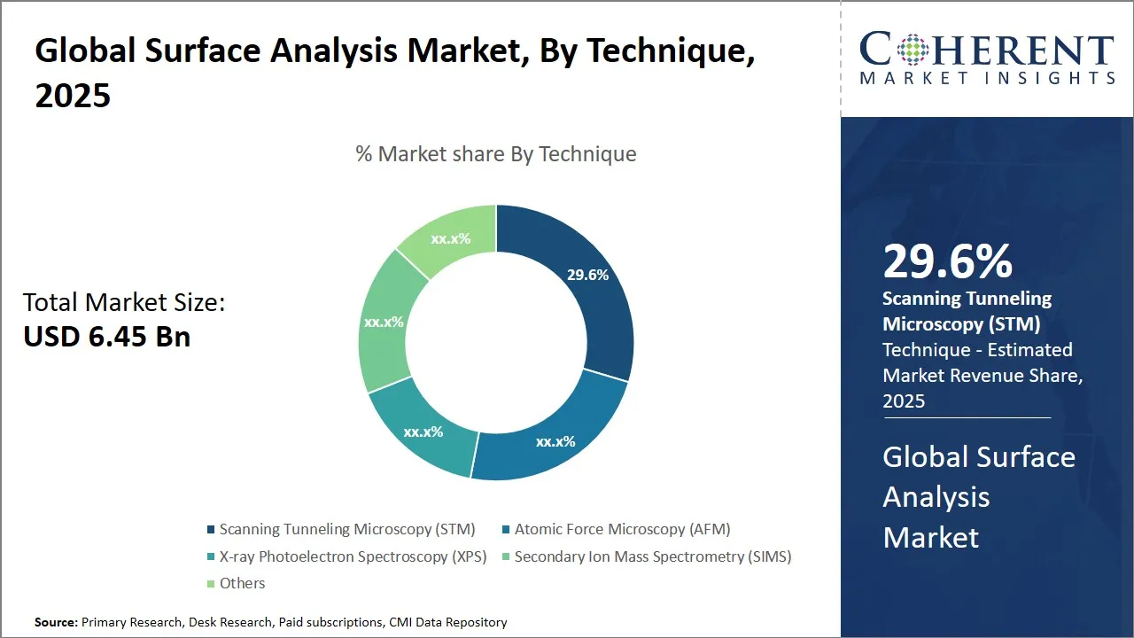
- Scanning Tunneling Microscopy (STM) segment is projected to account for 30.6% of the global surface analysis market share in 2026.
- The material science segment is expected to capture 24.8% of the surface analysis market share in 2026.
- The semiconductors segment is projected to hold 30.7% share in 2026.
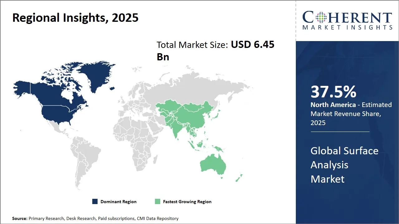
- North America is set to lead the global surface analysis market in 2026 with a 37.5% share. Asia Pacific, with a 23.5% share in 2026, is projected to be the fastest-growing region.
Market Overview
Market trends indicate a rising adoption of advanced surface analysis technologies such as atomic force microscopy and X-ray photoelectron spectroscopy, driven by the expanding semiconductor, automotive, and healthcare sectors. Additionally, the integration of AI and machine learning for data interpretation and automation is enhancing precision and efficiency, fueling the market expansion. Sustainability initiatives are also prompting more thorough surface evaluations to develop eco-friendly materials, further contributing to the sector’s growth trajectory.
Current Events and Its Impact
|
Current Events |
Description and its Impact |
|
NIST integrated testbeds and reference wafers for advanced metrology |
|
|
Canada instrumentation push via distributors |
|
Uncover macros and micros vetted on 75+ parameters: Get instant access to report
Surface Analysis Market Insights, By Technique - Scanning Tunneling Microscopy (STM) Segment Dominates the Market due to its Unparalleled Capability in Atomic-Scale Surface Characterization
Scanning Tunneling Microscopy (STM) is projected to hold 30.6% share in 2026, due to its ability to provide atomic-level resolution images of conductive material surfaces. This method allows scientists and industrial applications to learn the surface topographies and electronic characteristics with an incredible level of detail. The most important aspect that contributes to the development of STM is its exclusive principle of quantum tunneling which enables the measuring of surface irregularities and electron density maps which presents unmatched revelations over the properties of materials at the atomic level.
In materials science, STM has been crucial in visualizing the atomic arrangement of graphite surfaces. For example, researchers used STM to map the hexagonal lattice of graphite, directly observing individual carbon atoms and their electronic density variations. This capability enabled detailed studies of defects, adsorption sites, and surface reactions, establishing STM as a benchmark tool for nanotechnology and semiconductor surface characterization.
To learn more about this report, Download Free Sample
Surface Analysis Market Insights, By Application - Material Science Segment Dominates the Market due to its Critical Need for Material Innovation and Characterization
Material science segment is projected to account for 24.8% of the surface analysis market share in 2026, owing to the growing emphasis on developing advanced materials with tailored properties. Surface analysis is the foundation over which one can understand structure-property relationship; which is critical when developing materials to be used in particular applications such as strength, corrosion resistance, conductivity or catalytic activity can be achieved. New alloys, composite and thin films development is normally based on the advanced surface analysis techniques to determine the characterization of microstructures, surface morphology and chemical composition.
Surface Analysis Market Insights, By End-use Industry – Semiconductors Segment Dominates Propelled by Escalating Demand for Miniaturized and High-Performance Electronic Devices
The semiconductors segment is expected to capture 30.7% of the market share in 2026, due to its fervent requirements for precise control over surface and interface properties at the nanometer scale. Surface analysis is an essential tool to monitor and control thin films, dopant distributions, contamination and defect levels in semiconductor manufacturing processes, which are directly related to performance and reliability of the devices. Such a constant drive towards miniaturized, faster and energy saving electronics has required a high degree of surface characterization at both fabrication and quality control levels.
Regional Insights
To learn more about this report, Download Free Sample
North America Surface Analysis Market Analysis and Trends
The North America region is projected to lead the market with a 37.5% share in 2026. The region has a well-built ecosystem of the industry with a high level of concentration in the number of sophisticated research and development facilities, dominance of key semiconductor and materials science firms, and massive government funding in technology development. R&D offers various technologies in surface analysis that are applied in many industries such as electronics, aerospace, and healthcare that are continuously developed in the U.S. governments with the help of grants, subsidies, and favorable people policies.
Asia Pacific Surface Analysis Market Analysis and Trends
The Asia Pacific region is expected to exhibit the fastest growth in the market contributing 23.5% share in 2026, due to high industrialization trends, mass production capacity, and growing government research budgets of the emerging economies in China, Japan, and South Korea. The increasing industry of electronics, automobile and material production requires advanced surface analysis methods as a quality control and innovation tool.
The Made in China 2026 government policies, the advanced material research in Japan, and South Korea investments in nanotechnology have provided good platforms on which market can grow. The increasing popularity of the multinational companies as well as the highly competitive local companies like Rigaku Corporation, Horiba Ltd., and Shimadzu Corporation enhances the adoption of technology. More market dynamics are promoted by the trade liberalization and better intellectual property systems in the Asia Pacific which draw foreign investments and boost growth.
Surface Analysis Market Outlook for Key Countries
U.S. Surface Analysis Market Analysis and Trends
The U.S. surface analysis market is advantaged by an advanced industrial background whereby there are aerospace, electronics and biomedical industries that play a significant role. Major companies, such as Thermo Fisher Scientific and Agilent Technologies, are the ones that promote the innovation in the instruments and software of surface analysis.
Close partnerships between the federal government agencies like the Department of Energy and the corporate world enable the development of advanced technology. The programs of the government that encourage the development of the manufacturing industry and nanotechnology result in the demand of high-precision surface analysis devices that are necessary to develop products and ensure their quality.
Germany Surface Analysis Market Analysis and Trends
The automotive and industrial manufacturing dominate the world market is driving the surface analysis market of Germanys. The focus on precision engineering and surface quality in the country encourages the need to have sophisticated platforms of analysis. Such companies as Bruker Corporation which occupies great part of Germany surface analysis market takes an active role in market development providing special surface characterization tools which are used in automotive and materials science applications.
China Surface Analysis Market Analysis and Trends
The Chinese surface analysis market is developing at high rates due to large investments in semiconductor production, process of chemical processing and materials research. The policies that promote innovation in the country and growth in high-technological manufacturing centers form a solid foundation in the market growth. Large local players, who in most cases engage foreign companies like Rigaku Corporation and Horiba Ltd. are increasing their capabilities in surface analysis instruments. Non-protective trade policies and rising patent protection are other factors leading to a favorable business environment both to the emerging and established firms
Japan Surface Analysis Market Analysis and Trends
Japan has a high degree of sophistication in the areas of analytical instrumentation and firms such as Shimadzu Corporation and Horiba Ltd. have taken over the lead. The demand of surface analysis technologies is stabilized by the fact that the country is oriented on the highest attention to the manufacturing of products and materials. The interest of Japan in sustainable production and excellence in R&D stimulates the adoption of next-generation surface characterization in industry and in higher education. Recent incentives provided by governments to encourage innovation of nanotechnology and environmental monitoring also contribute to market growth.
South Korea Surface Analysis Market Analysis and Trends
South Korea’s dynamic electronics and semiconductor industries serve as key drivers for surface analysis technologies. With corporate giants such as Samsung and LG heavily investing in material characterization for product enhancement, the demand for surface analysis equipment remains strong. Local instrument manufacturers, often in partnership with global firms, are contributing to market growth through development of customized solutions catering to high-tech manufacturing. Government programs supporting innovation clusters and smart factories bolster uptake of advanced surface analysis technologies.
Regional Technological Readiness
|
Region/Country |
Government R&D signals directly relevant to surface metrology / nano-characterization |
|
European Union (incl. EU-27 NMIs via EURAMET) |
|
|
Japan |
|
Uncover macros and micros vetted on 75+ parameters: Get instant access to report
Macro and Micro Economic Factors Impacting on Surface Analysis Market Growth
Macroeconomic Factors Impacting Market Growth
- Government Programs and Environmental laws: Strict environmental laws by agencies such as EPA and WHO cause a demand in the surface analysis technologies to monitor and manage the contaminants particularly in manufacturing, pharmaceuticals and electronics. Regulatory compliance and sustainability requirements increase the market growth by facilitating the use of environmentally friendly analytical systems and environmentally friendly production methods.
- Policies in Public Health: The growing attention paid to the contamination prevention and hygiene across the globe and the tendency of the population to cities and ageing makes more and more people want surface analysis in the medical sector, food safety, and pharmaceutical industry. The regulatory organizations have stringent regulations, which demand sophisticated methods of characterizing surfaces.
- Funding and Economic Incentives: Economic incentives to support domestic manufacturing, research funding, and stimulus packages will help to improve innovation and market penetration of next-generation surface analysis instruments, including built-in smart technologies and AI-driven analytics.
Microeconomic Factors Impacting Growth
- Industry Specific Demand: The presence of increased adoption in industries such as semiconductor, electronics, pharmaceuticals, and materials science contributes to the necessity of the precision of the surface analysis, influenced by the trend such as miniaturization, automation, and non-destructive testing.
- Innovation in Technology: Innovations in the analysis methods, creation of new methods, i.e. atomic force microscopy, spectroscopy, in-situ analysis, multimodal imaging, and AI integration make the market more competitive and growing.
Instrument Manufacturers Offering AI-enabled Data Analysis Tools
|
Manufacturer |
Evidence |
|
JEO |
|
|
Bruker |
|
Uncover macros and micros vetted on 75+ parameters: Get instant access to report
Market Players, Key Development, and Competitive Intelligence
To learn more about this report, Download Free Sample
Key Developments
- In January 2025, Eurofins USA Environment Testing Eaton Analytical developed a cutting-edge method to detect chloronitramide anion, a newly discovered disinfection byproduct in drinking water, improving water quality analysis and safety. The innovation will make Eurofins Scientifics better skilled in surface and chemical testing by making it more proficient in the detection and assessment of contaminants, which cement its dominance in the domain of analytical testing in water and environmental safety.
- In July 2022, ULVAC-PHI launched PHI GENESIS, a fully automated XPS/HAXPES system designed for high-speed, high-sensitivity surface and interface analysis. This advancement strengthens Physical Electronics, Inc.'s position by enhancing automation, sensitivity, and analytical capabilities for metals, semiconductors, ceramics, and organic materials.
- In July 2024, Shimadzu Corporation joined forces with TESCAN Group to launch TESCAN's scanning electron microscopes in Japan this autumn, expanding its analytical measurement offerings. This partnership enhances Shimadzu’s surface analysis capabilities by combining TESCAN’s cutting-edge SEM technology with its existing instruments, enabling more precise and comprehensive material characterization.
Top Strategies Followed by Global Surface Analysis Market Players
- The existing competitors control the market through a high level of investment in research and development (R&D) to develop high-performance and technologically advanced surface analysis instruments. Also, these new entrants are engaged in aggressive international growth strategies through expansion of their distribution channels especially in the emerging markets where the line of surface analysis solution is experiencing rising demand. They can easily enter new areas of operation using their strong network and brand name and sign long term contracts with major clients.
- For example, Thermo Fisher developed the K Alpha X-ray Photoelectron Spectrometer (XPS) which improved the surface sensitivity, analysis throughput, which reinforces its pre-eminence in materials and nanotechnology studies.
- Surface analysis market players in the middle end tend to pursue strategies focused on providing low-end, but good enough solutions that would be appealing to cost-conscious consumers. These firms invest in the strike between the quality and affordability of the products, so catering to the large market segment of the targets comprising of the educational institutions, small and medium enterprises, and research laboratories that have small budgets. The middle-level players often form partnerships and collaborations to maximize their production processes and the uptake of technology to increase their market influence and technological capabilities.
- For example, companies like ULVAC-PHI, Rigaku Corporation, and HORIBA Scientific have implemented a value-based model through the provision of quality but affordable instruments. ULVAC-PHI specializes in cost-effective Auger electron spectroscopy (AES) and time of flight SIMS systems to universities and small research institutions.
- The surface analysis sector in the global human endeavors is highly competitive and the small players take a significantly different path in ensuring that they cut their own niche amidst the giants. They are more likely to focus on very specialized features or innovative solutions, which make them stand out of the larger competitors. The players serve niche applications and clients that require customized instrumentation by specializing in the latest technologies including miniaturized device, portable surface analyzers, or software-controlled analytical instruments.
- An example is the Kratos Analytical which offered AXIS Supra systems that are faster in sample throughput in research environments.
Market Report Scope
Surface Analysis Market Report Coverage
| Report Coverage | Details | ||
|---|---|---|---|
| Base Year: | 2025 | Market Size in 2026: | USD 6.80 Bn |
| Historical Data for: | 2020 To 2024 | Forecast Period: | 2026 To 2033 |
| Forecast Period 2026 to 2033 CAGR: | 5.4% | 2033 Value Projection: | USD 9.81 Bn |
| Geographies covered: |
|
||
| Segments covered: |
|
||
| Companies covered: |
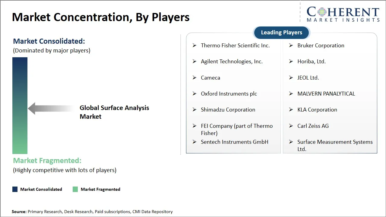
Thermo Fisher Scientific Inc., Bruker Corporation, Agilent Technologies, Inc., Horiba, Ltd., Cameca, JEOL Ltd., Oxford Instruments plc, MALVERN PANALYTICAL, Shimadzu Corporation, KLA Corporation, FEI Company (part of Thermo Fisher), Carl Zeiss AG, Sentech Instruments GmbH, and Surface Measurement Systems Ltd. |
||
| Growth Drivers: |
|
||
| Restraints & Challenges: |
|
||
Uncover macros and micros vetted on 75+ parameters: Get instant access to report
Surface Analysis Market Dynamics
To learn more about this report, Download Free Sample
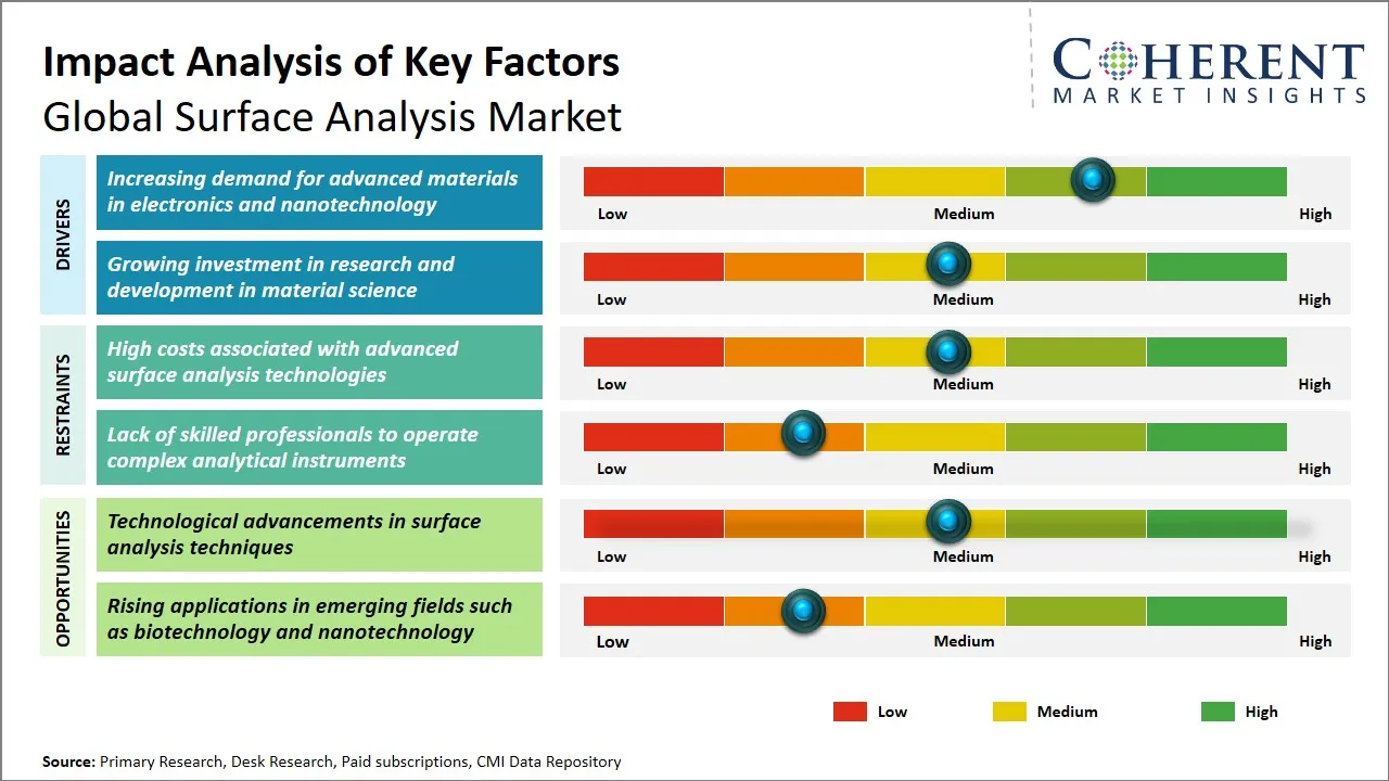
Surface Analysis Market Driver - Increasing Demand for Advanced Materials in Electronics and Nanotechnology
The growing demand of high-tech products in the electronics and nanotechnology industries is profoundly driving the use of the sophisticated surface studies in most parts of the world. With the ongoing development of electronic devices towards being smaller, faster and more complex, manufacturers are in need of very accurate characterization tools in order to investigate the surface properties of materials on the micro and nanoscale. This is especially important in the production of semiconductors, thin films and nanostructured surfaces, where surface flaws or fluctuations can significantly affect the device functionality and stability.
Samsung Electronics is an example and incorporates surface analysis into the manufacture of advanced semiconductor wafers. In the production of 3-nm and 5-nm chips, nanometer-level flaws are measured through atomic force microscopy (AFM) and X-ray photoelectron spectroscopy (XPS) to ensure that the surface composition is even.
Surface Analysis Market Opportunity - Technological Advancements in Surface Analysis Techniques
The global surface analysis Market will experience a significant growth occasioned by the high rate of technological changes in surface analysis methods. New technologies like high-resolution microscopy, better IR spectroscopy techniques and better imaging technology are providing the means of more accurate and detailed characterization of material surfaces. Several techniques such as time-of-flight secondary ion mass spectrometry (ToF-SIMS), Atomic Force Microscope and X-ray photoelectron spectroscopy (XPS) have been greatly improved in terms of sensitivity, resolution, and speed and can now provide a much more detailed analysis of surface composition and morphology at micro and nano scales.
Analyst Opinion (Expert Opinion)
- The global surface analysis market is experiencing noteworthy growth, driven by advancements in nanotechnology and increasing demand for high-precision analytical tools. Insights from the Surface Analysis Conference (2023) and the International Conference on Nanoscience and Nanotechnology (2022) highlighted key developments, with companies like Bruker and Horiba spearheading innovations in surface characterization techniques.
- Bruker's recent launch of a state-of-the-art atomic force microscope exemplifies the focus on enhancing resolution and speed, catering specifically to the needs of materials science and semiconductor industries. Discussions at these conferences underscored the rising importance of surface analysis in developing advanced materials, particularly in the automotive and electronics sectors.
- The challenges such as high costs associated with advanced equipment and the need for skilled personnel were frequently mentioned as potential barriers to market penetration. Companies that prioritize user-friendly interfaces and offer comprehensive training programs will likely gain a competitive edge. Furthermore, strategic collaborations with research institutions can foster innovation.
Market Segmentation
- Technique Insights (Revenue, USD Bn, 2021 - 2033)
- Scanning Tunneling Microscopy (STM)
- Atomic Force Microscopy (AFM)
- X-ray Photoelectron Spectroscopy (XPS)
- Secondary Ion Mass Spectrometry (SIMS)
- Others
- Application Insights (Revenue, USD Bn, 2021 - 2033)
- Material Science
- Nanotechnology
- Biotechnology
- Electronics
- Others
- End-use Industry Insights (Revenue, USD Bn, 2021 - 2033)
- Semiconductors
- Healthcare
- Automotive
- Aerospace
- Others
- Regional Insights (Revenue, USD Bn, 2021 - 2033)
- North America
- U.S.
- Canada
- Latin America
- Brazil
- Argentina
- Mexico
- Rest of Latin America
- Europe
- Germany
- U.K.
- Spain
- France
- Italy
- Russia
- Rest of Europe
- Asia Pacific
- China
- India
- Japan
- Australia
- South Korea
- ASEAN
- Rest of Asia Pacific
- Middle East
- GCC Countries
- Israel
- Rest of Middle East
- Africa
- South Africa
- North Africa
- Central Africa
- North America
- Key Players Insights
- Thermo Fisher Scientific Inc.
- Bruker Corporation
- Agilent Technologies, Inc.
- Horiba, Ltd.
- Cameca
- JEOL Ltd.
- Oxford Instruments plc
- MALVERN PANALYTICAL
- Shimadzu Corporation
- KLA Corporation
- FEI Company (part of Thermo Fisher)
- Carl Zeiss AG
- Sentech Instruments GmbH
- Surface Measurement Systems Ltd.
Sources
Primary Research Interviews
- Director of R&D – Leading Surface Analysis Instrument Manufacturer
- Head of Procurement – Major Analytical Laboratory Chain
- Product Development Lead – Prominent Material Science Company
- Quality Assurance Manager – Industrial Coatings Manufacturer
Stakeholders
- Manufacturers of Surface Analysis Instruments (e.g., XPS, AES, SIMS, AFM, SEM and related systems)
- End-use Sectors
- Electronics & Semiconductors
- Automotive & Aerospace Components
- Energy & Battery Manufacturers
- Pharmaceuticals & Biotechnology Companies
- Academic and Research Institutes
- Industrial Coatings and Thin Film Manufacturers
- Regulatory and Accreditation Bodies (ISO, ASTM, national standards bodies)
- E-commerce and Distribution Platforms for Scientific Equipment
- Technology Solution Providers: Automation/AI/Software Integration for Analysis & Imaging
Databases
- UN Comtrade Database (International trade of analytical and scientific instruments)
- India Import Export (EXIM) Database (Scientific instrumentation flows in India)
- USITC DataWeb (U.S. analytical instrumentation import/export data)
Magazines
- Analytical Scientist – Innovations and trends in surface analysis
- Instrument Business Outlook – Market insights for analytical instrumentation
- Materials Today – Application updates in material and surface characterization
- Lab Manager Magazine – End-user trends in laboratory instrumentation
Journals
- Surface Science (Elsevier) – Advances in surface analysis techniques and applications
- Journal of Vacuum Science & Technology – Research in vacuum-based surface analysis
- Applied Surface Science – Studies on surface and interface characterization
- Journal of Materials Science – Analytical developments for materials research
Newspapers
- The Financial Times – Coverage of global analytical instrumentation markets
- The Wall Street Journal – Business trends impacting scientific equipment and R&D sectors
- Nikkei Asia – Asia-Pacific region trends in instrumentation and material sciences
Associations
- American Vacuum Society (AVS)
- International Union for Vacuum Science, Technique and Applications (IUVSTA)
- Federation of Analytical Chemistry and Spectroscopy Societies (FACSS)
- International Organization for Standardization (ISO)
- European Materials Research Society (E-MRS)
Public Domain Sources
- U.S. Food and Drug Administration (FDA) – Device guidelines for analytical/laboratory instrumentation
- European Commission – REACH Regulations, Scientific Instrument Directives
- World Health Organization (WHO) – Laboratory standards and protocols
Proprietary Elements
- CMI Data Analytics Tool, Proprietary CMI Existing Repository of information for last 8 years.
Share
Share
About Author
Yash Doshi is a Senior Management Consultant. He has 12+ years of experience in conducting research and handling consulting projects across verticals in APAC, EMEA, and the Americas.
He brings strong acumen in helping chemical companies navigate complex challenges and identify growth opportunities. He has deep expertise across the chemicals value chain, including commodity, specialty and fine chemicals, plastics and polymers, and petrochemicals. Yash is a sought-after speaker at industry conferences and contributes to various publications on topics related commodity, specialty and fine chemicals, plastics and polymers, and petrochemicals.
Missing comfort of reading report in your local language? Find your preferred language :
Transform your Strategy with Exclusive Trending Reports :
Frequently Asked Questions
EXISTING CLIENTELE
Joining thousands of companies around the world committed to making the Excellent Business Solutions.
View All Our Clients