

Global Memory Interface Chip Market Size and Forecast – 2026 To 2033
The global memory interface chip market is expected to grow from USD 6.80 Bn in 2026 to USD 13.90 Bn by 2033, registering a compound annual growth rate (CAGR) of 8% from 2026 to 2033. The global memory interface chip market is driven by the expansion of hyperscale cloud data centers. On September 23, 2025, OpenAI, Oracle, and SoftBank announced five new U.S. AI data center sites under Stargate, OpenAI’s overarching AI infrastructure platform. The combined capacity from these five new site brings Stargate to nearly 7 gigawatts of planned capacity and over USD 400 billion in investment over the next three years.
Key Takeaways of the Global Memory Interface Chip Market
- The Memory Buffer Chips segment is expected to account for 36.0% of the global memory interface chip market share in 2026. Increasing demand for high-performance computing infrastructure is driving the growth of the segment. On December 13, 2024, The Leibniz Supercomputing Center (LRZ) of the Bavarian Academy of Sciences and Humanities commissioned Hewlett Packard Enterprise to build its next high-performance computer, called Blue Lion.
- The DDR segment is estimated to capture 33.0% of the market share in 2026. Expansion of HBM-enabled AI accelerators is majorly driving the growth of the segment. On March 18, 2024, NVIDIA announced the launch of the NVIDIA Blackwell platform, enabling organizations everywhere to build and run real-time generative AI on trillion-parameter large language models at up to 25x less cost and energy consumption than its predecessor.
- The Data Centers segment is estimated to capture 26.0% of the market share in 2026. Rapid growth of enterprise storage and networking equipment is driving the growth of the segment. On April 9, 2026, Lenovo Group Limited announced it has completed the acquisition of Infinidat Ltd., a global provider of high-end enterprise storage solutions. The transaction strengthens Lenovo’s position in enterprise storage and enhances its ability to deliver resilient, intelligent, AI-ready data infrastructure to customers worldwide.
- North America is expected to dominate the memory interface chip market in 2026 with a market share of 41.0%. Rising automotive demand for high-speed memory connectivity in North America is driving the growth of the regional market. On October 22, 2024, Qualcomm introduced the Snapdragon Ride Elite platform for software-defined vehicles, integrating high-performance AI processing with support for LPDDR5X memory to power advanced driver assistance systems, autonomous driving, and digital cockpit applications.
- Asia Pacific is expected to account for 30.0% of the market share in 2026 and is projected to record the fastest growth over the forecast period. Growing investments in edge AI servers and industrial computing across Asia Pacific is driving the growth of the regional market. On July 16, 2026, Advantech released its AIR series Edge AI server portfolio for industrial automation, smart manufacturing and machine vision applications in Taiwan, Japan, South Korea and Southeast Asia
- Growing Integration of CXL Memory Expansion for AI Servers: Memory interface chip makers are accelerating the development of CXL-compliant memory controllers and buffer chips to support memory pooling, memory expansion and lower latency in AI servers and hyperscale data centers, thereby enabling next-generation GPU clusters and large language model
- Rapid Transition Toward DDR5 and High-Bandwidth Memory Ecosystems: The industry is experiencing rapid adoption of DDR5 Register Clock Drivers (RCDs), Data Buffer Chips (DBCs), and High-Bandwidth Memory (HBM) interface solutions as AI accelerators, enterprise servers, and high-performance computing platforms demand much higher bandwidth and better power efficiency.
Segmental Insights
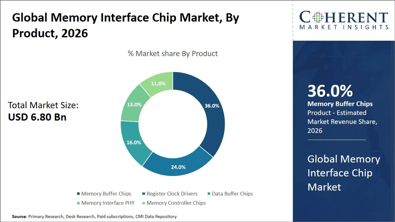
Why Do Memory Buffer Chips Dominate the Global Memory Interface Chip Market?
The memory buffer chips segment is expected to account for 36.0% of the global memory interface chip market share in 2026. Memory buffer chips are crucial for increasing memory capacity and enhancing signal integrity on today’s server and data center architectures. In enterprise systems, buffer chips play a key role in maintaining reliable communication between processors and multiple memory modules when adopting DDR5 and high-density memory configurations to support artificial intelligence, cloud computing, and high-performance computing workloads. They also help improve scalability and overall system performance. On April 22, 2026, JEDEC Solid State Technology Association previewed a set of new features planned for incorporation into the next version of its JESD209‑6 LPDDR6 standard. Building on the foundational JESD209‑6 published in July 2025, JEDEC’s JC‑42.6 Subcommittee has been working to enhance the next version of the standard to extend LPDDR6 beyond mobile platforms to support selected data center and accelerated computing workloads seeking a power‑efficient, high‑capacity memory platform.
- Current Industry Events of 2026
- Market Size Estimation
- Regional Breakdown
- Competitive Landscape
- Customer Intelligence
- Segmental Analysis
- Pricing Analysis
- Key Market Drivers, Challenges & Future Trends
- Customized Insights Section
Why is DDR the Most Preferred Memory Technology?
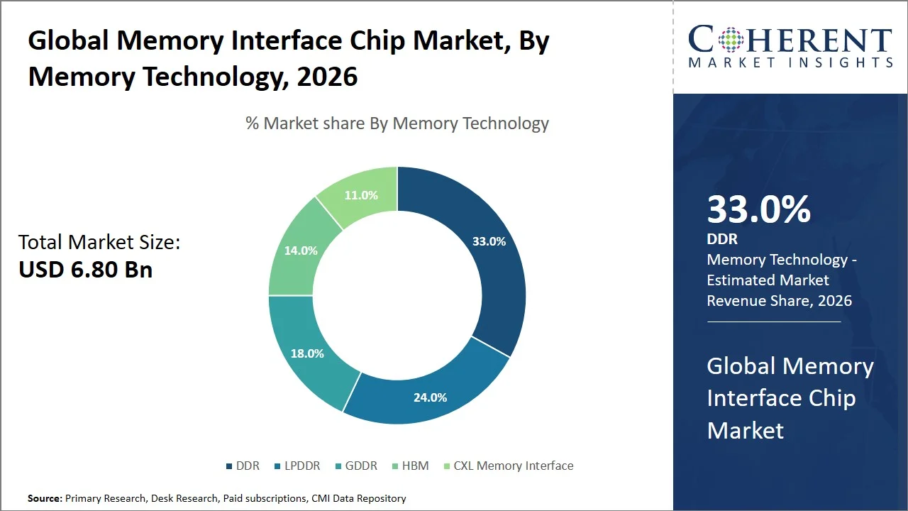
The DDR segment is expected to account for 33.0% of the global memory interface chip market share in 2026. The DDR memory technology remains the most desired because it delivers the best balance of performance, compatibility and cost on a wide spectrum of computing platforms. The continuous evolution from DDR4 to DDR5 has brought substantial enhancements in memory bandwidth, better power efficiency, and higher memory capacity, with ongoing ecosystem support from processor vendors, server providers, and memory module manufacturers. DDR remains the go-to option for data centers, enterprise systems, personal computers, and industrial computing applications. On February 24, 2025, Intel announced the Xeon 6300 series (Xeon 6 entry-server processors), which have native DDR5-4800 ECC memory support that enables increased memory bandwidth and better platform compatibility for enterprise servers and edge computing deployments. The launch further solidified DDR5 as the memory technology of choice for today’s server infrastructure.
Data Centers Dominate the Global Memory Interface Chip Market
The data centers segment is expected to account for 34.0% of the global memory interface chip market share in 2026. Memory interface chips are predominantly used in data centers, which have the highest need for memory bandwidth, low latency, and huge memory subsystems for AI training, cloud computing, virtualization, and high-performance computing workloads. Advanced memory interface components such as register clock drivers, data buffers and memory controllers are becoming more and more importance in modern servers to provide reliable data transmission, effective memory scaling and continuous operation in densely packed multi-processor server systems. On July 20, 2026, Micron and Meta announced LPCAMM2 LPDDR5X server memory designed for AI data centers, which cuts memory power consumption to about one-third of that of traditional DDR5 and improves bandwidth-per-watt for hyperscale AI applications.
Current Events and their Impact
Current Events | Description and its Impact |
European Union - European Chips Act |
|
United States - CHIPS and Science Act Implementation |
|
Global Memory Interface Chip Market Dynamics
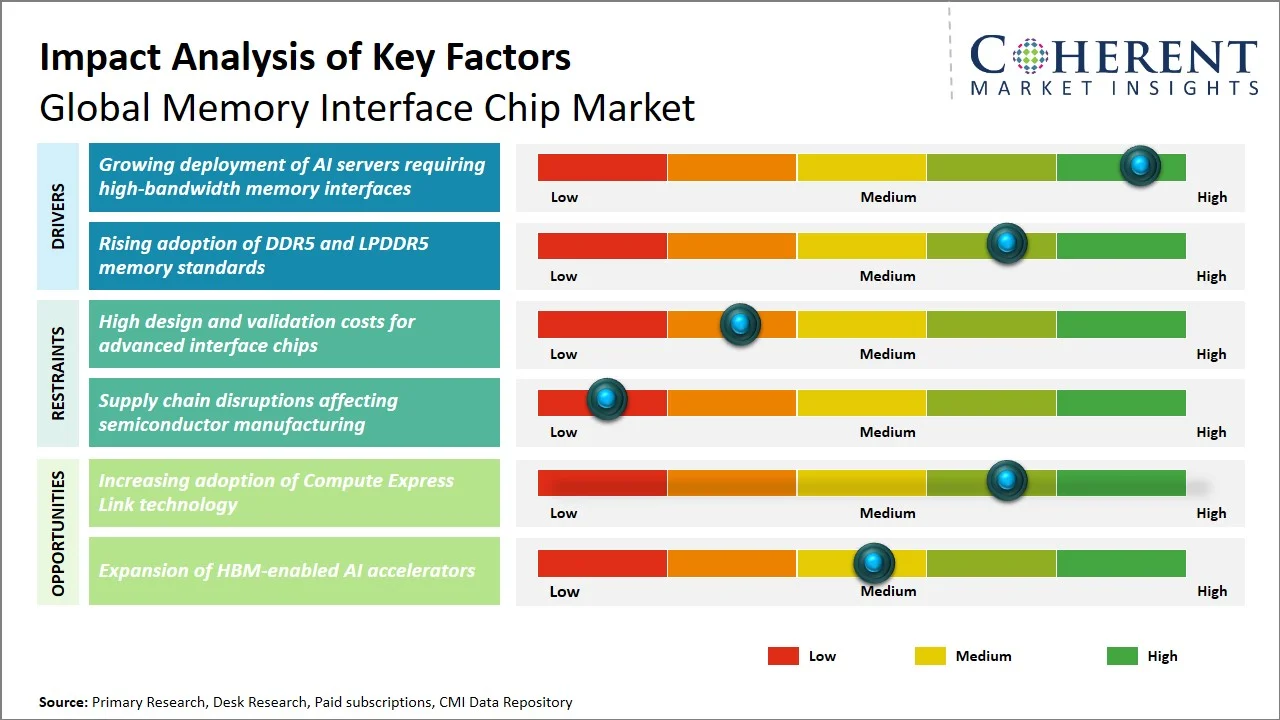
Market Drivers
Growing deployment of AI servers requiring high-bandwidth memory interfaces
The rapidly growing artificial intelligence infrastructure is creating a huge need for memory interface chips that can support exceptionally high data transfer rates between processors and memory modules. AI servers are increasingly deploying high-bandwidth memory, DDR5 and Compute Express Link-compatible architectures with advanced GPUs and AI accelerators that demand sophisticated register clock drivers, memory buffers and interface controllers to optimize signal integrity, reduce latency and enable scalable memory configurations for large language models, generative AI and high-performance computing workloads. On June 12, 2025, AMD launched the AMD Instinct MI350 Series, delivering up to 4x generation-on-generation AI compute improvement and up to 35x leap in inferencing performance. The company also previewed its next-gen “Helios” AI reference design rack integrating AMD Instinct MI400 GPUs, EPYC Venice CPUs, and Pensando Vulcano NICs for unprecedented AI compute density and scalability.
Rising adoption of DDR5 and LPDDR5 memory standards
The mass migration from legacy memory technologies to DDR5 and LPDDR5 is resulting in a strong demand for sophisticated memory interface chips that offer higher bandwidth, higher memory density, and better power efficiency. As the next generation memory standards are rapidly being adopted across enterprise servers, personal computers, AI platforms, automotive electronics and high-end consumer devices, semiconductor makers are developing optimized interface solutions to support reliable communication, faster data transfer and better system performance. On May 7, 2025, Gigabyte, G.SKILL, Kingston and TeamGroup unveiled DDR5 CAMM2 memory solutions at ComputeX 2025, showcasing high-speed DDR5 modules geared for future desktop and mobile platforms.
Emerging Trends
Advanced Packaging and Chiplet-Based Memory Architectures
Semiconductor companies are increasingly integrating memory interface chips with chiplet-based processors via 2.5D and 3D advanced packaging technologies that are capable of delivering higher signal integrity, lower interconnect latency, and improved scalability for data center processors and AI accelerators.
Rising Deployment of Low-Power Memory Interface Solutions for Edge AI
Chip vendors are developing very power-efficient memory interface chips optimized for LPDDR5X and the next-generation LPDDR6 architectures to drive edge AI devices, autonomous systems, industrial automation equipment and intelligent networking platforms where both performance and energy efficiency are critical.
Regional Insights
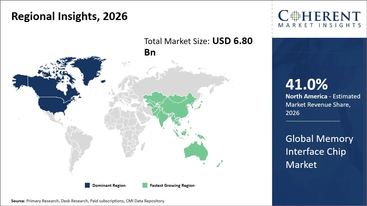
Why is North America a Strong Market for Memory Interface Chips?
North America is expected to account for a market share of 41.0% in 2026. North America will remain the primary region for innovation in memory interface chips, with AI accelerator developers, hyperscale cloud providers and interface IP businesses concentrated in the region. Rambus, Astera Labs, Cadence Design Systems, Synopsys, AMD, Intel, NVIDIA, and Marvell Technology are among the industry leaders in the US that are working on memory interface solutions for the DDR5, HBM3E and Compute Express Link (CXL) ecosystems.
Meanwhile, the Blackwell GPU platform from NVIDIA has HBM3E memory with sophisticated memory interfaces for AI training clusters, while AMD’s Instinct MI350 series and Intel’s Xeon 6 processors offer high-capacity DDR5 and CXL memory extension. Leading hyperscale operators like Microsoft Azure, Amazon Web Services, Google Cloud and Meta are continuing to construct AI data centers employing memory-rich server architectures that require register clock drivers, memory buffers and high-speed PHY solutions. The region also enjoys significant semiconductor R&D investment through the CHIPS and Science Act, expediting innovative packaging and chiplet integration.
Why Does the Asia Pacific Memory Interface Chip Market Exhibit High Growth?
Asia Pacific is projected to account for 30.0% of the global memory interface chip market in 2026 and is expected to register the fastest growth. The Asia Pacific region has the world’s largest semiconductor manufacturing ecosystem for memory interface chips, due to its sophisticated memory fabrication, OSAT capabilities, semiconductor equipment manufacture, and electronics manufacturing. The mass manufacture of DDR5, LPDDR5X, GDDR7 and HBM devices that demand complex interface chips has been cooperatively backed by Samsung Electronics, SK hynix, Micron Taiwan, TSMC, UMC and several packaging businesses. South Korea is the world’s top HBM maker, Taiwan leads in advanced logic production and CoWoS packaging, Japan provides semiconductor materials and equipment, and China is rapidly building out domestic memory manufacturing capacity with YMTC and CXMT. The region also houses the world’s largest electronics manufacturing centers, supplying servers, AI accelerators, networking equipment, smartphones and industrial computer platforms that increasingly incorporate next generation memory interfaces.
Global Memory Interface Chip Market Outlook for Key Countries
Why is the U.S. Emerging as a Major Hub in the Memory Interface Chip Market?
The U.S. is the global center for memory interface chip architecture, IP development, and AI server platform design. Rambus is at the forefront of DDR5 register clock drivers and memory interface chips, while Astera Labs has successfully shipped CXL memory connectivity products that have gained broad adoption in hyperscale AI infrastructure. Semiconductor firms globally use high-speed DDR5, LPDDR5X, HBM3E and CXL interface IP from Cadence Design Systems and Synopsys. NVIDIA, AMD, Intel, Broadcom, and Marvell are continuing to release AI CPUs that support HBM3E and advanced memory interconnects that need sophisticated interface technology. Microsoft, Oracle, Amazon Web Services, Google and Meta continue to invest in large-scale AI infrastructure, and the rising use of servers with multiple terabytes of DDR5 memory and CXL memory extension is helping to drive demand for memory interface components.
Is China the Next Growth Engine for the Memory Interface Chip Market?
With government-backed semiconductor localization efforts and higher output of memory devices, China is rapidly building a domestic memory interface chip ecosystem. With ChangXin Memory Technologies’ accelerated production of DDR5 DRAM and Yangtze Memory Technologies’ ramping of NAND flash production, compatible interface solutions are emerging in the local supply chain. Huawei, Biren Technology, Cambricon and Hygon are pushing out AI processors and server platforms that employ high-speed memory architectures, using advanced memory controllers and interface technologies. Chinese cloud providers such as Alibaba Cloud, Tencent Cloud, Baidu AI Cloud and Huawei Cloud are continuing to deploy AI computing clusters based on domestic and international hardware, driving increased need for high-performance memory connectivity solutions. Further helping the country’s integrated memory ecosystem are major expenditures in semiconductor equipment, packaging and testing capabilities.
Japan Memory Interface Chip Market Analysis and Trends
Japan’s strength in semiconductor materials and semiconductor production equipment, and research in memory technology, strategically positions it well in the memory interface chip market. Renesas Electronics is developing memory controller and interface solutions for automotive, industrial and embedded applications. Kioxia continues to innovate in enterprise SSD technologies that rely on high-speed memory architectures. Tokyo Electron, SCREEN Holdings, Canon, Nikon, and Advantest supply critical semiconductor manufacturing and testing equipment used globally for producing advanced memory interface devices. Rapidus is also building next-generation semiconductor manufacturing capabilities supported by government funding and collaborations with leading global technology partners. Japanese car manufacturers are using more AI-enabled computing systems with LPDDR5 and DDR5 memory architectures for autonomous driving and software defined vehicle platforms.
Taiwan Memory Interface Chip Market Analysis and Trends
Taiwan dominates the globe in advanced memory interface chip manufacture, based on its leadership in semiconductor foundry services and advanced packaging. TSMC produces high-performance CPUs and interface chips for NVIDIA, AMD, Broadcom, Marvell and many other fabless semiconductor businesses using leading-edge process nodes. The company has significantly ramped up CoWoS advanced packaging capability to meet the increasing HBM integration in AI accelerators, in turn benefiting demand for complex memory interface technologies. MediaTek keeps on adding LPDDR5X interfaces to high-end mobile chipsets. Winbond Electronics and Nanya Technology produce specialist DRAM for industrial and embedded applications. ASE Technology and SPIL further bolster Taiwan’s position as a provider of superior semiconductor packaging and testing services that are vital for high-speed memory interface solutions.
South Korea Memory Interface Chip Market Analysis and Trends
South Korea is a key player in the worldwide memory interface chip ecosystem with Samsung Electronics and SK hynix leading the way in advanced DRAM and HBM manufacturing. Samsung has commercialized HBM3E memory for next-generation AI accelerators and continues to enhance its sophisticated packaging technology. SK hynix is also a key provider of HBM utilized in NVIDIA AI GPUs. Both firms are aggressively ramping production of DDR5, LPDDR5X, GDDR7 and HBM products that require advanced register clock drivers, memory buffers and signal integrity solutions. Packaging businesses, substrate makers and equipment vendors are working under the government’s K-Semiconductor Strategy to help strengthen the country’s semiconductor ecosystem. South Korea is also investing in AI semiconductor development, advanced packaging facilities and next-generation memory research, further solidifying its leadership across the global memory interface chip value chain.
Global Memory Interface Chip Market - Compute Express Link (CXL) Controller and Memory Expander Adoption Analysis
Deployment Category | Estimated Adoption Share (2025) | Primary End Users | Typical CXL Device Type |
Direct-attached CXL memory expansion controllers | 71% | Hyperscale cloud providers | Type 3 Memory Expander |
Memory pooling controllers | 13% | AI server manufacturers | Type 3 Memory Pool |
CXL switch and fabric controllers | 8% | Enterprise data centers | Fabric Switch |
CXL memory appliances | 5% | High-performance computing centers | Memory Appliance |
Custom CXL controller ASICs | 3% | GPU cluster operators | Proprietary Type 3 Controller |
How is the Increasing Adoption of Compute Express Link Technology Creating New Growth Opportunities in the Memory Interface Chip Market?
The rising use of Compute Express Link (CXL) technology is generating new growth prospects in the memory interface chip market by boosting demand for specialized CXL memory controllers, retimers, switches and memory expansion buffer chips used in AI and cloud server systems. Intel Xeon 6 processors, AMD EPYC Turin platforms and AI systems based on the new NVIDIA Blackwell architecture are being designed with CXL support to enable memory pooling, memory tiering and disaggregated memory infrastructure, letting multiple processors and accelerators share large DDR5 memory resources across a server rack.
Companies such as Astera Labs have commercialized CXL connectivity products for hyperscale deployments, while Rambus and other interface vendors are developing CXL-compatible memory subsystem solutions for next-generation AI servers. As hyperscale operators deploy memory expansion shelves and composable infrastructure to support large language model training and inference workloads, the requirement for high-speed CXL interface chips with low latency, signal integrity management, and scalable memory interconnect capability is expanding significantly, creating a new product category beyond traditional DDR memory interface components.
On January 22, 2026, Astera Labs, Inc. announced an expanded portfolio roadmap that will feature new capabilities, including support for increased radix, platform-specific protocols, in-network computing, Hypercast technology, and optical connectivity. Close collaboration with hyperscale customers and initial platform deployments have revealed new opportunities for the merchant scale-up switching market which is projected to reach USD 20 billion by 2030.
Market Players, Key Development, and Competitive Intelligence
Key Developments
- On June 21, 2026, Intel announced a series of data center advancements, including new Intel Xeon 6+ processors, an expanded 800 Series Ethernet portfolio featuring the Intel Ethernet E835 controllers and network adapters, and continued progress on its AI accelerator roadmap, including updates on Crescent Island.
- On May 26, 2026, Rambus Inc. announced its complete DDR5 9600 Client Memory Module Chipset for high-performance CUDIMM, CQDIMM and CSODIMM modules in future generation AI PCs. The chipset includes the new Gen2 Client Clock Driver (CKD02), delivering breakthrough performance with support for PC memory module operation of up to 9600 MT/s, Power Management IC (PMIC5120) and Serial Presence Detect Hub (SPD Hub).
Competitive Landscape
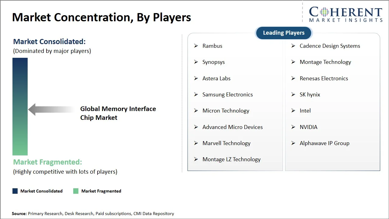
The memory interface chip market is led by Rambus, Astera Labs, Cadence Design Systems, Synopsys, Montage Technology, and Renesas Electronics, with competition increasingly centered on AI server memory architectures, CXL connectivity, and high-speed DDR5/HBM interfaces rather than conventional memory controllers. Rambus has strengthened its position by expanding its DDR5 Register Clock Driver (RCD), Client Clock Driver (CKD), and HBM memory interface IP portfolio for enterprise servers and AI accelerators, while Astera Labs has rapidly gained traction through its CXL Smart Connectivity Platform, including Aries Smart Retimers, Leo Memory Connectivity Controllers, and Scorpio Fabric Switches designed for GPU clusters.
Cadence and Synopsys continue to deliver DDR5, LPDDR5X, HBM3E and CXL PHY/IP solutions to top semiconductor firms building specialized AI CPUs. Montage Technology continues to be a leading provider of DDR5 RCDs and data buffer chips for server DIMMs, especially for Asia data center installations. Renesas Electronics focuses on high-reliability memory interface solutions for industrial and automotive applications. Increasing collaboration between interface IP providers, foundries such as TSMC, advanced packaging companies, and AI processor vendors has shifted competition toward delivering complete memory connectivity ecosystems optimized for next-generation AI infrastructure.
Market Report Scope
Memory Interface Chip Market Report Coverage
| Report Coverage | Details | ||
|---|---|---|---|
| Base Year: | 2025 | Market Size in 2026: | USD 6.80 Bn |
| Historical Data for: | 2020 To 2024 | Forecast Period: | 2026 To 2033 |
| Forecast Period 2026 to 2033 CAGR: | 8% | 2033 Value Projection: | USD 13.90 Bn |
| Geographies covered: |
| ||
| Segments covered: |
| ||
| Companies covered: | Rambus, Cadence Design Systems, Synopsys, Montage Technology, Astera Labs, Renesas Electronics, Samsung Electronics, SK hynix, Micron Technology, Intel, Advanced Micro Devices, NVIDIA, Marvell Technology, Alphawave IP Group, and Montage LZ Technology | ||
| Growth Drivers: |
| ||
| Restraints & Challenges: |
| ||
Analyst Opinion (Expert Opinion)
- The future of the industry is expected to be defined by coherent memory architectures rather than simply faster memory speeds. As hyperscale AI clusters continue scaling from thousands to tens of thousands of GPUs, memory interface chips supporting CXL, HBM4, DDR6, and optical interconnect compatibility are expected to become essential components of every AI server platform, significantly increasing semiconductor content per server.
- The strongest opportunity is expected to emerge in CXL memory interface chips for AI data center applications in the United States, where hyperscale cloud providers are rapidly deploying memory-disaggregated server architectures. The concentration of premier AI processor, memory, and semiconductor manufacturing ecosystems is projected to provide further high-growth possibilities in the HBM interface solutions for AI accelerators in South Korea and DDR5 register clock drivers for corporate servers made in Taiwan.
- Market participants should make expenditures for CXL 3.x controllers, HBM4 interface IP, chiplet-ready memory PHYs and advanced packaging compatibility, rather than only competing on standard DDR interface solutions. “Next-generation AI infrastructure platforms will have longer qualification cycles, but product lifecycles and margins are significantly higher. Strategic partnerships with AI GPU developers, hyperscale cloud operators, memory manufacturers and advanced packaging providers will be key to securing design wins.
Speak to the analyst
Want personalized insights?
Take the findings above to one of our principal consultants, or have the report rebuilt around the segments, geographies and competitors you actually track.
Market Segmentation
- Product Insights (Revenue, USD Billion, 2021 - 2033)
- Memory Buffer Chips
- Register Clock Drivers
- Data Buffer Chips
- Memory Interface PHY
- Memory Controller Chips
- Memory Technology Insights (Revenue, USD Billion, 2021 - 2033)
- DDR
- LPDDR
- GDDR
- HBM
- CXL Memory Interface
- Application Insights (Revenue, USD Billion, 2021 - 2033)
- Data Centers
- Consumer Electronics
- Automotive
- Industrial
- Telecommunications
- High Performance Computing
- Regional Insights (Revenue, USD Billion, 2021 - 2033)
- North America
- U.S.
- Canada
- Latin America
- Brazil
- Argentina
- Mexico
- Rest of Latin America
- Europe
- Germany
- U.K.
- Spain
- France
- Italy
- Russia
- Rest of Europe
- Asia Pacific
- China
- India
- Japan
- Australia
- South Korea
- ASEAN
- Rest of Asia Pacific
- Middle East
- GCC Countries
- Israel
- Rest of Middle East
- Africa
- South Africa
- North Africa
- Central Africa
- North America
Sources
Primary Research Interviews
- Semiconductor distributors and channel partners
- Data center infrastructure operators
- Semiconductor packaging and OSAT companies
- Enterprise storage and networking equipment manufacturers
Magazines
- IEEE Spectrum
- IEEE Solid-State Circuits Magazine
- Semiconductor Engineering
- EE Times
Journals
- IEEE Journal of Solid-State Circuits
- IEEE Transactions on Circuits and Systems
- IEEE Transactions on Very Large Scale Integration (VLSI) Systems
- IEEE Transactions on Computer-Aided Design of Integrated Circuits and Systems
Associations
- JEDEC Solid State Technology Association
- Compute Express Link (CXL) Consortium
- Semiconductor Industry Association (SIA)
- SEMI
Public Domain Sources
- U.S. Securities and Exchange Commission (SEC) filings
- JEDEC DDR5, LPDDR5, LPDDR6, and HBM standards documentation
- Compute Express Link (CXL) Consortium technical specifications
- Semiconductor Industry Association (SIA) reports
Proprietary Elements
- CMI Data Analytics Tool
- Proprietary CMI Existing Repository of Information for the Last 10 Years
Get access to 250+ pages report
Every segment, forecast, competitor profile and data table behind the analysis above — available for instant download.
- ESOMAR Member
- ISO 9001:2015 Certified
- D-U-N-S Registered
- GDPR & CCPA Compliant
Missing comfort of reading report in your local language? Find your preferred language:
Transform your Strategy with Exclusive Trending Reports
Frequently Asked Questions
The global memory interface chip market is expected to stand at USD 6.80 Bn in 2026 and is expected to reach USD 13.90 Bn by 2033.
The CAGR of the global memory interface chip market is projected to be 8% from 2026 to 2033.
Growing deployment of AI servers requiring high-bandwidth memory interfaces and rising adoption of DDR5 and LPDDR5 memory standards are the major factors driving the growth of the global memory interface chip market.
High design and validation costs for advanced interface chips and supply chain disruptions affecting semiconductor manufacturing are the major factors hampering the growth of the global memory interface chip market.
In terms of product, the memory buffer chips segment is estimated to dominate the market revenue share in 2026.
Maintaining signal integrity ensures reliable high-speed data transmission between processors and memory modules.
They distribute clock signals accurately across DDR memory modules to improve timing performance.